- 您現在的位置:買賣IC網 > PDF目錄373982 > ADF4193BCPZ (ANALOG DEVICES INC) Low Phase Noise, Fast Settling PLL Frequency Synthesizer PDF資料下載
參數資料
| 型號: | ADF4193BCPZ |
| 廠商: | ANALOG DEVICES INC |
| 元件分類: | XO, clock |
| 英文描述: | Low Phase Noise, Fast Settling PLL Frequency Synthesizer |
| 中文描述: | PLL FREQUENCY SYNTHESIZER, 3500 MHz, QCC32 |
| 封裝: | 5 X 5 MM, ROHS COMPLIANT, MO-220VHHD-2, LFCSP-32 |
| 文件頁數: | 20/28頁 |
| 文件大小: | 437K |
| 代理商: | ADF4193BCPZ |
第1頁第2頁第3頁第4頁第5頁第6頁第7頁第8頁第9頁第10頁第11頁第12頁第13頁第14頁第15頁第16頁第17頁第18頁第19頁當前第20頁第21頁第22頁第23頁第24頁第25頁第26頁第27頁第28頁
ADF4193
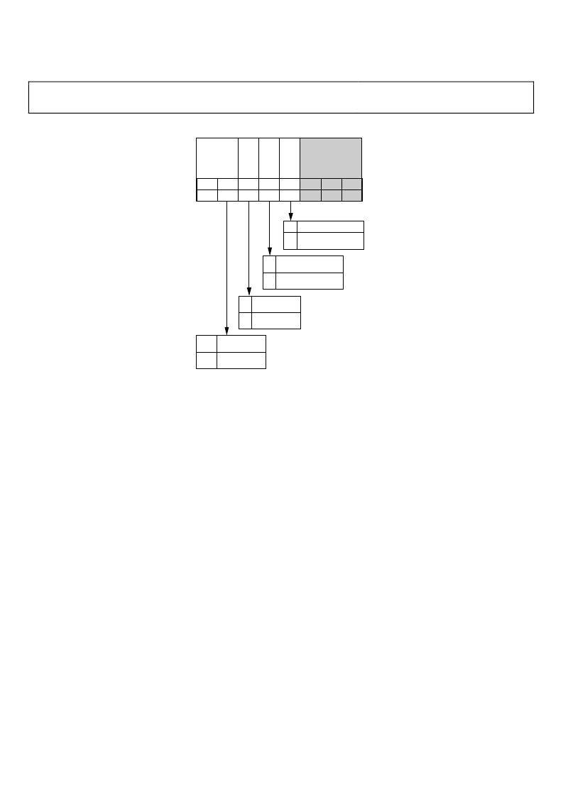
POWER-DOWN REGISTER (R5)
Rev. B | Page 20 of 28
0
DB7
F5
DB6
F4
DB5
F3
DB4
F2
DB3
F1
DB2
C3 (1)
DB1
C2 (0)
DB0
C1 (1)
C
R
C
3
P
C
P
CONTROL
BITS
PD
DIFF AMP
0
1
F4
0
1
F5
DISABLED
ENABLED
DIFF AMP
POWER-DOWN
0
1
F2
NORMAL OPERATION
3-STATE ENABLED
CHARGE PUMP
3-STATE
0
1
F1
NORMAL OPERATION
COUNTER RESET
COUNTER RESET
0
1
F3
DISABLED
ENABLED
CHARGE PUMP
POWER-DOWN
Figure 34. Power-Down Register (R5)
R5, the power-down register (C3, C2, C1 set to 1, 0, 1,
respectively) can be used to software power down the PLL and
differential amplifier sections. After power is initially applied,
there must be writes to R5 to clear the power-down bits and to
R2, R1, and R0 before the ADF4193 comes out of power-down.
Power-Down Differential Amplifier
When Bit DB6 and Bit DB7 are set high, the differential
amplifier is put into power-down. When Bit DB6 and Bit DB7
are set low, normal operation is resumed.
Power-Down Charge Pump
Setting Bit DB5 high activates a charge pump power-down and
the following events occur:
All active dc current paths are removed, except for the
differential amplifier.
The R and N divider counters are forced to their load state
conditions.
The charge pump is powered down with its outputs in three-
state mode.
The digital lock detect circuitry is reset.
The RF
IN
input is debiased.
The reference input buffer circuitry is disabled.
The serial interface remains active and capable of loading and
latching data.
For normal operation, Bit DB5 should be set to 0, followed by a
write to R0.
CP Three-State
When this bit is set high, the charge pump outputs are put into
three-state. With the bit set low, the charge pump outputs are
enabled.
Counter Reset
When this bit is set to 1, the counters are held in reset. For
normal operation, this bit should be 0, followed by a write to R0.
相關PDF資料 |
PDF描述 |
|---|---|
| ADF4193BCPZ-RL | Low Phase Noise, Fast Settling PLL Frequency Synthesizer |
| ADF4193BCPZ-RL7 | Low Phase Noise, Fast Settling PLL Frequency Synthesizer |
| ADF4207BRU | Dual RF PLL Frequency Synthesizers |
| ADF4208BRU | Dual RF PLL Frequency Synthesizers |
| ADF4206 | Dual RF PLL Frequency Synthesizers |
相關代理商/技術參數 |
參數描述 |
|---|---|
| ADF4193BCPZ-RL | 功能描述:IC PLL FREQ SYNTHESIZER 32LFCSP RoHS:是 類別:集成電路 (IC) >> 時鐘/計時 - 時鐘發生器,PLL,頻率合成器 系列:- 標準包裝:2,000 系列:- 類型:PLL 時鐘發生器 PLL:帶旁路 輸入:LVCMOS,LVPECL 輸出:LVCMOS 電路數:1 比率 - 輸入:輸出:2:11 差分 - 輸入:輸出:是/無 頻率 - 最大:240MHz 除法器/乘法器:是/無 電源電壓:3.135 V ~ 3.465 V 工作溫度:0°C ~ 70°C 安裝類型:表面貼裝 封裝/外殼:32-LQFP 供應商設備封裝:32-TQFP(7x7) 包裝:帶卷 (TR) |
| ADF4193BCPZ-RL7 | 功能描述:IC PLL FREQ SYNTHESIZER 32LFCSP RoHS:是 類別:集成電路 (IC) >> 時鐘/計時 - 時鐘發生器,PLL,頻率合成器 系列:- 標準包裝:2,000 系列:- 類型:PLL 時鐘發生器 PLL:帶旁路 輸入:LVCMOS,LVPECL 輸出:LVCMOS 電路數:1 比率 - 輸入:輸出:2:11 差分 - 輸入:輸出:是/無 頻率 - 最大:240MHz 除法器/乘法器:是/無 電源電壓:3.135 V ~ 3.465 V 工作溫度:0°C ~ 70°C 安裝類型:表面貼裝 封裝/外殼:32-LQFP 供應商設備封裝:32-TQFP(7x7) 包裝:帶卷 (TR) |
| ADF4193SP1BCPZ | 制造商:Analog Devices 功能描述: |
| ADF4193SP1BCPZ-RL7 | 制造商:Analog Devices 功能描述: |
| ADF4193SP2BCPZ-RL7 | 制造商:Analog Devices 功能描述: |
發布緊急采購,3分鐘左右您將得到回復。