- 您現在的位置:買賣IC網 > PDF目錄374019 > ADP3166JRU-REEL (ANALOG DEVICES INC) 5-Bit Programmable 2-, 3-, 4-Phase Synchronous Buck Controller PDF資料下載
參數資料
| 型號: | ADP3166JRU-REEL |
| 廠商: | ANALOG DEVICES INC |
| 元件分類: | 穩壓器 |
| 英文描述: | 5-Bit Programmable 2-, 3-, 4-Phase Synchronous Buck Controller |
| 中文描述: | SWITCHING CONTROLLER, 4000 kHz SWITCHING FREQ-MAX, PDSO28 |
| 封裝: | TSSOP-28 |
| 文件頁數: | 17/20頁 |
| 文件大小: | 351K |
| 代理商: | ADP3166JRU-REEL |
REV. 0
ADP3166
–17–
to further derate the capacitor, or to choose a capacitor rated at
a higher temperature than required. Several capacitors may be
placed in parallel to meet size or height requirements in the
design. In this example, the input capacitor bank is formed by
three 2200
μ
F, 16 V Nichicon capacitors with a ripple current
rating of 3.5 A each.
To reduce the input-current di/dt to below the recommended
maximum of 0.1 A/
μ
s, an additional small inductor (L > 1
μ
H
@ 15 A) should be inserted between the converter and the sup-
ply bus. That inductor also acts as a filter between the converter
and the primary power source.
R
= R
V
V
(
–V
–V
CS2 NEW
CS2 OLD
NL
FLCOLD
NL
FLHOT
)
)
×
(
)
)
(35)
TUNING PROCEDURE FOR ADP3166
1.
Build a circuit based on compensation values computed
from the design spreadsheet.
2.
Hook up the dc load to the circuit, turn it on, and verify its
operation. Also check for jitter at no load and full load.
DC Loadline Setting
3.
Measure the output voltage at no load (V
NL
). Verify that
it is within tolerance.
4.
Measure the output voltage at full load cold (V
FLCOLD
). Let
the board set for a ~10 minutes at full load and measure
output (V
FLHOT
). If there is a change of more than a few
millivolts, adjust R
CS1
and R
CS2
using Equations 35 and 37.
5.
Repeat Step 4 until the cold and hot voltage measurements
remain the same.
6.
Measure the output voltage from no load to full load using 5
A steps. Compute the loadline slope for each change and
then average them to get the overall loadline slope (R
OMEAS
).
7.
If
R
OMEAS
is off by more than 0.05 m
from
R
O
, use Equa-
tion 36 to adjust the
R
PH
values:
R
R
8.
Repeat Steps 6 and 7 to check the loadline and repeat the
adjustments if necessary.
9.
Once finished with dc loadline adjustment, do not change
R
PH
, R
CS1
, R
CS2
, or R
TH
for the rest of the procedure.
10.
Measure the output ripple at no load and at full load with
a scope and make sure that it is within spec.
R
= R
PH NEW
PH OLD
OMEAS
O
)
)
(36)
AC Loadline Setting
11.
Remove the dc load from the circuit and hook up the
dynamic load.
12.
Hook up the scope to the output voltage and set it to dc
coupling with the time scale at 100
μ
s/div.
13.
Set the dynamic load for a transient step of about 24 A at 1
kHz with 50% duty cycle.
14.
Measure the output waveform (it might be necessary to
use a dc offset on scope to see the waveform). Try to use a
vertical scale of 100 mV/div or finer.
15.
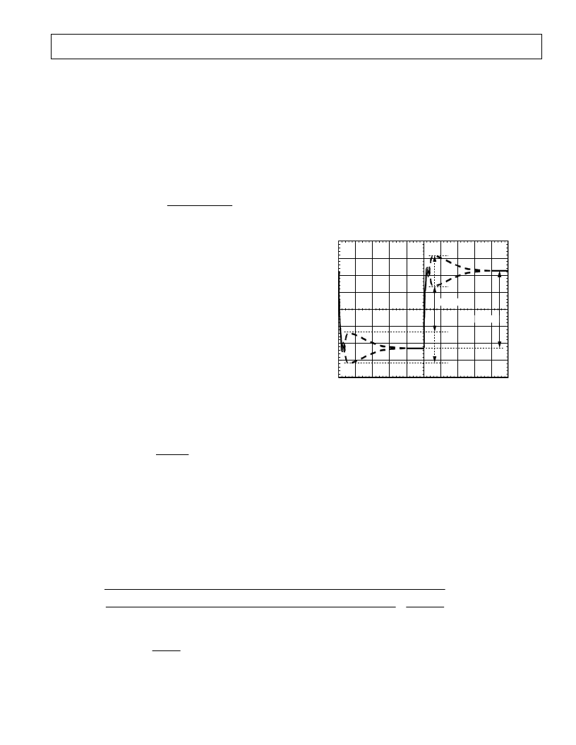
The waveform should look something like Figure 3. Use
the horizontal cursors to measure V
ACDRP
and V
DCDRP
as shown. DO NOT MEASURE THE UNDER
SHOOT
OR OVERSHOOT THAT HAPPENS
IMMEDI-
ATELY AFTER THE STEP.
V
ACDRP
V
DCDRP
Figure 3. AC Loadline Waveform
If the V
ACDRP
and V
DCDRP
are different by more than a few
millivolts, use the following to adjust C
CS
. It might be
necessary to parallel different values to get the right one
since there are limited standard capacitor values available.
(It is a good idea to have locations for two capacitors in
the layout for this.)
Repeat Steps 11 to 13 and repeat adjustments if neces-
sary. Once complete, do not change C
CS
for the rest of
the procedure.
Set the dynamic load step to maximum step size (do not
use a step size larger than needed), and verify that the
output waveform is square (meaning V
ACDRP
and V
DCDRP
are equal).
16.
17.
18.
R
=
R
+R
R
R
+ R
(
– R
R
– R
–R
CS
NEW
CS OLD
1
TH
C
CS OLD
1
TH
C
CS
OLD
CS2 NEW
OLD
TH
C
TH
C
2
25
25
2
1
25
25
1
(
1
(
)
)
)
)
×
)
(
)
(
)
)
(
)
(
)
(
)
×
o
o
o
o
CS
(37)
C
= C
V
V
CS NEW
CS OLD
ACDRP
DCDRP
)
)
(38)
相關PDF資料 |
PDF描述 |
|---|---|
| ADP3166JRU-REEL7 | 5-Bit Programmable 2-, 3-, 4-Phase Synchronous Buck Controller |
| ADP3170JRU | VRM 8.5 Compatible Single Phase Core Controller |
| ADP3170 | Charger front end protection IC with 30V max Vin and 4.5V LDO output 8-WSON 0 to 125 |
| ADP3171JR | Charger front end protection IC with 30V max Vin and 4.5V LDO output 8-WSON 0 to 125 |
| ADP3171 | Charger front end protection IC with 30V max Vin and 4.5V LDO output 8-WSON 0 to 125 |
相關代理商/技術參數 |
參數描述 |
|---|---|
| ADP3166JRU-REEL7 | 功能描述:IC REG BUCK 5BIT 2-4PHAS 28TSSOP RoHS:否 類別:集成電路 (IC) >> PMIC - 穩壓器 - 專用型 系列:- 產品培訓模塊:Lead (SnPb) Finish for COTS Obsolescence Mitigation Program 標準包裝:2,000 系列:- 應用:電源,ICERA E400,E450 輸入電壓:4.1 V ~ 5.5 V 輸出數:10 輸出電壓:可編程 工作溫度:-40°C ~ 85°C 安裝類型:表面貼裝 封裝/外殼:42-WFBGA,WLCSP 供應商設備封裝:42-WLP 包裝:帶卷 (TR) |
| ADP3166JRUZ-REEL | 功能描述:IC REG BUCK 5BIT 2-4PHAS 28TSSOP RoHS:是 類別:集成電路 (IC) >> PMIC - 穩壓器 - 專用型 系列:- 產品培訓模塊:Lead (SnPb) Finish for COTS Obsolescence Mitigation Program 標準包裝:2,000 系列:- 應用:電源,ICERA E400,E450 輸入電壓:4.1 V ~ 5.5 V 輸出數:10 輸出電壓:可編程 工作溫度:-40°C ~ 85°C 安裝類型:表面貼裝 封裝/外殼:42-WFBGA,WLCSP 供應商設備封裝:42-WLP 包裝:帶卷 (TR) |
| ADP3167 | 制造商:未知廠家 制造商全稱:未知廠家 功能描述:ADP3160/ADP3167: 5-Bit Programmable 2-Phase Synchronous Buck Controller Data Sheet (Rev. B. 5/02) |
| ADP3167JR | 制造商:Rochester Electronics LLC 功能描述:- Bulk |
| ADP3167JR-REEL7 | 制造商:Rochester Electronics LLC 功能描述:5BIT PROG'BLE 2 PHASE SYNCRO BUCK CNTRLR - Tape and Reel |
發布緊急采購,3分鐘左右您將得到回復。