- 您現在的位置:買賣IC網 > PDF目錄374019 > ADP3166JRU-REEL (ANALOG DEVICES INC) 5-Bit Programmable 2-, 3-, 4-Phase Synchronous Buck Controller PDF資料下載
參數資料
| 型號: | ADP3166JRU-REEL |
| 廠商: | ANALOG DEVICES INC |
| 元件分類: | 穩壓器 |
| 英文描述: | 5-Bit Programmable 2-, 3-, 4-Phase Synchronous Buck Controller |
| 中文描述: | SWITCHING CONTROLLER, 4000 kHz SWITCHING FREQ-MAX, PDSO28 |
| 封裝: | TSSOP-28 |
| 文件頁數: | 6/20頁 |
| 文件大小: | 351K |
| 代理商: | ADP3166JRU-REEL |
REV. 0
–6–
ADP3166
PIN FUNCTION DESCRIPTIONS
Pin No. Mnemonic
Function
1–5
VID4–VID0
Voltage Identification DAC Inputs. These five pins are pulled up to an internal reference, providing a
logic 1 if left open. When in normal operation mode, the DAC output programs the FB regulation voltage
from 0.8 V to 1.55 V. Leaving VID4 through VID0 open results in the ADP3166 going into a “No CPU”
mode, shutting off its PWM outputs.
Crowbar Output. This logic-level output can be used to control an external device to short the 12 V supply
to ground to protect the CPU from overvoltage if CSREF exceeds 2.1 V.
Feedback Return. VID DAC and error amplifier reference for remote sensing of the output voltage.
Feedback Input. Error amplifier input for remote sensing of the output voltage. A resistor between this pin
and the output voltage sets the no-load offset point.
Error Amplifier Output and Compensation Point.
Power Good Output. Open-drain output that pulls to GND when the output voltage is outside of the
proper operating range.
Power Supply Enable Input. Pulling this pin to GND disables the PWM outputs.
Soft Start Delay and Current Limit Latch-Off Delay Setting Input. A resistor and capacitor connected
between this pin and GND sets the soft start ramp-up time and the overcurrent latch-off delay time.
Frequency Setting Resistor Input. An external resistor connected between this pin and GND sets the oscil-
lator frequency of the device.
PWM Ramp Current Input. A resistor from the converter input voltage to this pin sets the internal PWM ramp.
Current Limit Set Point/Enable Output. A resistor from this pin to GND sets the current limit threshold of
the converter. This pin is actively pulled low when the ADP3166 EN input is low, or when VCC is below
its UVLO threshold to signal to the driver IC that the driver high-side and low-side outputs should go low.
Current Sense Reference Voltage Input. The voltage on this pin is used as the reference for the current
sense amplifiers and the Power Good and Crowbar functions. This pin should be connected to the com-
mon point of the output inductors.
Current Sense Summing Node. Resistors from each switch node to this pin sum the average inductor cur-
rents together to measure the total output current.
Current Sense Compensation Point. A resistor and capacitor from this pin to CSSUM determine the slope
of the load line and the positioning loop response time.
Ground. All internal biasing and the logic output signals of the device are referenced to this ground.
Current Balance Inputs. Inputs for measuring the current level in each phase. The SW pins of unused
phases should be grounded.
PWM4–PWM1 Logic-Level PWM Outputs. Each output is connected to the input of an external MOSFET driver such
as the ADP3413 or ADP3418. Connecting the PWM3 and/or PWM 4 outputs to GND will cause that
phase to turn off, allowing the ADP3166 to operate as a 2-, 3-, or 4-phase controller.
VCC
Supply Voltage for the Device.
6
CROWBAR
7
8
FBRTN
FB
9
10
COMP
PWRGD
11
12
EN
DELAY
13
RT
14
15
RAMPADJ
ILIMIT
16
CSREF
17
CSSUM
18
CSCOMP
19
20–23
GND
SW4–SW1
24–27
28
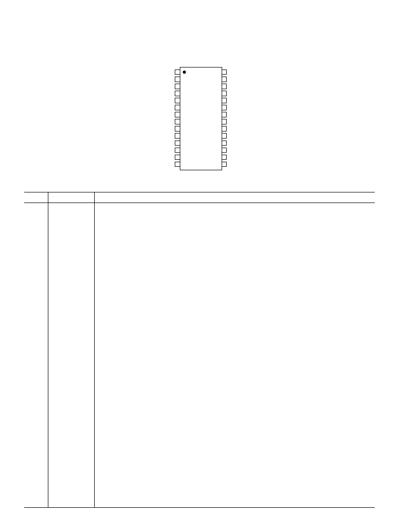
PIN CONFIGURATION
RU-28
ADP3166
TOP VIEW
(Not to Scale)
VID4
VCC
VID3
PWM1
VID2
PWM2
VID1
PWM3
VID0
PWM4
CROWBAR
SW1
FBRTN
SW2
FB
SW3
COMP
SW4
PWRGD
GND
EN
CSCOMP
DELAY
CSSUM
RT
CSREF
RAMPADJ
ILIMIT
1
2
3
28
27
26
4
8
10
12
14
5
6
7
21
24
23
22
9
11
17
18
19
13
15
16
20
25
相關PDF資料 |
PDF描述 |
|---|---|
| ADP3166JRU-REEL7 | 5-Bit Programmable 2-, 3-, 4-Phase Synchronous Buck Controller |
| ADP3170JRU | VRM 8.5 Compatible Single Phase Core Controller |
| ADP3170 | Charger front end protection IC with 30V max Vin and 4.5V LDO output 8-WSON 0 to 125 |
| ADP3171JR | Charger front end protection IC with 30V max Vin and 4.5V LDO output 8-WSON 0 to 125 |
| ADP3171 | Charger front end protection IC with 30V max Vin and 4.5V LDO output 8-WSON 0 to 125 |
相關代理商/技術參數 |
參數描述 |
|---|---|
| ADP3166JRU-REEL7 | 功能描述:IC REG BUCK 5BIT 2-4PHAS 28TSSOP RoHS:否 類別:集成電路 (IC) >> PMIC - 穩壓器 - 專用型 系列:- 產品培訓模塊:Lead (SnPb) Finish for COTS Obsolescence Mitigation Program 標準包裝:2,000 系列:- 應用:電源,ICERA E400,E450 輸入電壓:4.1 V ~ 5.5 V 輸出數:10 輸出電壓:可編程 工作溫度:-40°C ~ 85°C 安裝類型:表面貼裝 封裝/外殼:42-WFBGA,WLCSP 供應商設備封裝:42-WLP 包裝:帶卷 (TR) |
| ADP3166JRUZ-REEL | 功能描述:IC REG BUCK 5BIT 2-4PHAS 28TSSOP RoHS:是 類別:集成電路 (IC) >> PMIC - 穩壓器 - 專用型 系列:- 產品培訓模塊:Lead (SnPb) Finish for COTS Obsolescence Mitigation Program 標準包裝:2,000 系列:- 應用:電源,ICERA E400,E450 輸入電壓:4.1 V ~ 5.5 V 輸出數:10 輸出電壓:可編程 工作溫度:-40°C ~ 85°C 安裝類型:表面貼裝 封裝/外殼:42-WFBGA,WLCSP 供應商設備封裝:42-WLP 包裝:帶卷 (TR) |
| ADP3167 | 制造商:未知廠家 制造商全稱:未知廠家 功能描述:ADP3160/ADP3167: 5-Bit Programmable 2-Phase Synchronous Buck Controller Data Sheet (Rev. B. 5/02) |
| ADP3167JR | 制造商:Rochester Electronics LLC 功能描述:- Bulk |
| ADP3167JR-REEL7 | 制造商:Rochester Electronics LLC 功能描述:5BIT PROG'BLE 2 PHASE SYNCRO BUCK CNTRLR - Tape and Reel |
發布緊急采購,3分鐘左右您將得到回復。