- 您現在的位置:買賣IC網 > PDF目錄374019 > ADP3166JRU-REEL (ANALOG DEVICES INC) 5-Bit Programmable 2-, 3-, 4-Phase Synchronous Buck Controller PDF資料下載
參數資料
| 型號: | ADP3166JRU-REEL |
| 廠商: | ANALOG DEVICES INC |
| 元件分類: | 穩壓器 |
| 英文描述: | 5-Bit Programmable 2-, 3-, 4-Phase Synchronous Buck Controller |
| 中文描述: | SWITCHING CONTROLLER, 4000 kHz SWITCHING FREQ-MAX, PDSO28 |
| 封裝: | TSSOP-28 |
| 文件頁數: | 18/20頁 |
| 文件大小: | 351K |
| 代理商: | ADP3166JRU-REEL |
REV. 0
–18–
ADP3166
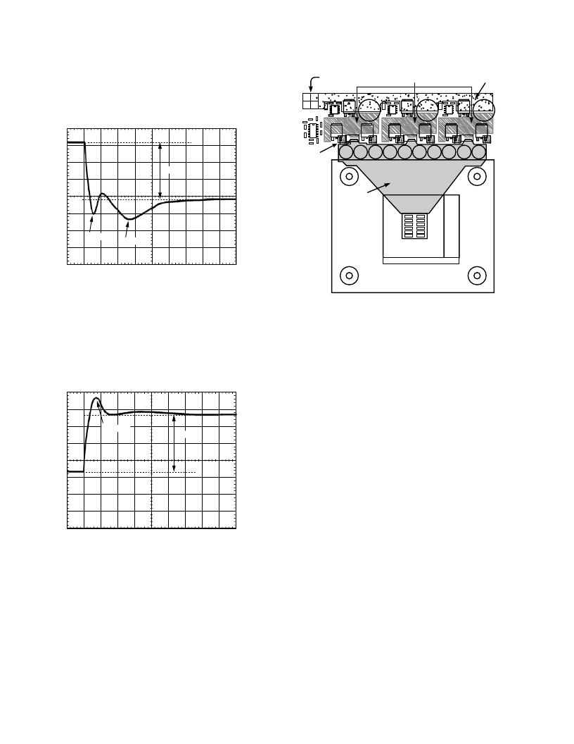
Initial Transient Setting
19.
With dynamic load still set at maximum step size, expand
scope time scale to see 2
μ
s/div to 5
μ
s/div. The waveform
may have two overshoots and one minor undershoot (see
Figure 5). Here, V
DROOP
is the final desired static value.
V
DROOP
V
TRAN1
V
TRAN2
Figure 4. Transient Setting Waveform
If the overshoots are larger than desired, try making the
following adjustments in this order (Note: if these adjust-
ments do not change the response, you are limited by the
output decoupling). Check the output response each time
a change is made as well as the switching nodes (to make
sure it is still stable).
a. Make the ramp resistor larger by 25% (R
RAMP
).
b.
For V
TRAN1
, increase CB or switching frequency.
c. For V
TRAN2
, increase RA and decrease C
A
by 25%.
20.
V
DROOP
V
TRANREL
Figure 5. Transient Setting Waveform
For load release (see Figure 5), if VTRANREL is larger
than V
TRAN1
(refer to Figure 4), there is not enough
output capacitance. Either more capacitance is needed or
it is necessary to make the inductor values smaller (if
inductors are changed, it is necessary to start design over
using the spreadsheet and this tuning guide).
21.
LAYOUT AND COMPONENT PLACEMENT
The following guidelines are recommended for optimal performance
of a switching regulator in a PC system. Key layout issues are
illustrated in Figure 6.
12V CONNECTOR
INPUT POWER PLANE
THERMISTOR
OUTPUT
POWER
PLANE
CPU
SOCKET
KEEP-OUT
AREA
KEEP-OUT
AREA
SWITCH NODE
PLANES
KEEP-OUT
AREA
KEEP-OUT
AREA
Figure 6. Layout Recommendations
General Recommendations
For good results, at least a four-layer PCB is recommended.
This should allow the needed versatility for control circuitry
interconnections with optimal placement, power planes for
ground, input and output power, and wide interconnection
traces in the rest of the power delivery current paths. Keep
in mind that each square unit of 1 ounce copper trace has a
resistance of ~0.53 m
at room temperature.
Whenever high currents must be routed between PCB lay-
ers, vias should be used liberally to create several parallel
current paths so that the resistance and inductance intro-
duced by these current paths is minimized and the via current
rating is not exceeded.
If critical signal lines (including the output voltage sense
lines of the ADP3166) must cross through power circuitry,
it is best if a signal ground plane can be interposed between
those signal lines and the traces of the power circuitry. This
serves as a shield to minimize noise injection into the signals
at the expense of making signal ground a bit noisier.
An analog ground plane should be used around and under
the ADP3166 for referencing the components associated
with the controller. This plane should be tied to the nearest
output decoupling capacitor ground and should not be tied
to any other power circuitry to prevent power currents from
flowing in it.
The components around the ADP3166 should be located
close to the controller with short traces. The most important
traces to keep short and away from other traces are the FB
and CSSUM pins. Refer to Figure 6 for more details on
layout for the CSSUM node.
The output capacitors should be connected as close as
possible to the load (or connector) that receives the power
(e.g., a microprocessor core). If the load is distributed, the
capacitors should also be distributed, and generally in pro-
portion to where the load tends to be more dynamic.
Avoid crossing any signal lines over the switching power
path loop, described below.
相關PDF資料 |
PDF描述 |
|---|---|
| ADP3166JRU-REEL7 | 5-Bit Programmable 2-, 3-, 4-Phase Synchronous Buck Controller |
| ADP3170JRU | VRM 8.5 Compatible Single Phase Core Controller |
| ADP3170 | Charger front end protection IC with 30V max Vin and 4.5V LDO output 8-WSON 0 to 125 |
| ADP3171JR | Charger front end protection IC with 30V max Vin and 4.5V LDO output 8-WSON 0 to 125 |
| ADP3171 | Charger front end protection IC with 30V max Vin and 4.5V LDO output 8-WSON 0 to 125 |
相關代理商/技術參數 |
參數描述 |
|---|---|
| ADP3166JRU-REEL7 | 功能描述:IC REG BUCK 5BIT 2-4PHAS 28TSSOP RoHS:否 類別:集成電路 (IC) >> PMIC - 穩壓器 - 專用型 系列:- 產品培訓模塊:Lead (SnPb) Finish for COTS Obsolescence Mitigation Program 標準包裝:2,000 系列:- 應用:電源,ICERA E400,E450 輸入電壓:4.1 V ~ 5.5 V 輸出數:10 輸出電壓:可編程 工作溫度:-40°C ~ 85°C 安裝類型:表面貼裝 封裝/外殼:42-WFBGA,WLCSP 供應商設備封裝:42-WLP 包裝:帶卷 (TR) |
| ADP3166JRUZ-REEL | 功能描述:IC REG BUCK 5BIT 2-4PHAS 28TSSOP RoHS:是 類別:集成電路 (IC) >> PMIC - 穩壓器 - 專用型 系列:- 產品培訓模塊:Lead (SnPb) Finish for COTS Obsolescence Mitigation Program 標準包裝:2,000 系列:- 應用:電源,ICERA E400,E450 輸入電壓:4.1 V ~ 5.5 V 輸出數:10 輸出電壓:可編程 工作溫度:-40°C ~ 85°C 安裝類型:表面貼裝 封裝/外殼:42-WFBGA,WLCSP 供應商設備封裝:42-WLP 包裝:帶卷 (TR) |
| ADP3167 | 制造商:未知廠家 制造商全稱:未知廠家 功能描述:ADP3160/ADP3167: 5-Bit Programmable 2-Phase Synchronous Buck Controller Data Sheet (Rev. B. 5/02) |
| ADP3167JR | 制造商:Rochester Electronics LLC 功能描述:- Bulk |
| ADP3167JR-REEL7 | 制造商:Rochester Electronics LLC 功能描述:5BIT PROG'BLE 2 PHASE SYNCRO BUCK CNTRLR - Tape and Reel |
發布緊急采購,3分鐘左右您將得到回復。