- 您現在的位置:買賣IC網 > PDF目錄374039 > ADUC702 (Analog Devices, Inc.) 5 AMP MINIATURE POWER RELAY PDF資料下載
參數資料
| 型號: | ADUC702 |
| 廠商: | Analog Devices, Inc. |
| 英文描述: | 5 AMP MINIATURE POWER RELAY |
| 中文描述: | 精密模擬微控制器的12位模擬I / O,ARM7TDMI的微控制器 |
| 文件頁數: | 21/80頁 |
| 文件大小: | 840K |
| 代理商: | ADUC702 |
第1頁第2頁第3頁第4頁第5頁第6頁第7頁第8頁第9頁第10頁第11頁第12頁第13頁第14頁第15頁第16頁第17頁第18頁第19頁第20頁當前第21頁第22頁第23頁第24頁第25頁第26頁第27頁第28頁第29頁第30頁第31頁第32頁第33頁第34頁第35頁第36頁第37頁第38頁第39頁第40頁第41頁第42頁第43頁第44頁第45頁第46頁第47頁第48頁第49頁第50頁第51頁第52頁第53頁第54頁第55頁第56頁第57頁第58頁第59頁第60頁第61頁第62頁第63頁第64頁第65頁第66頁第67頁第68頁第69頁第70頁第71頁第72頁第73頁第74頁第75頁第76頁第77頁第78頁第79頁第80頁
Preliminary Technical Data
ADuC702x Series
MEMORY ORGANISATION
Rev. PrB | Page 21 of 80
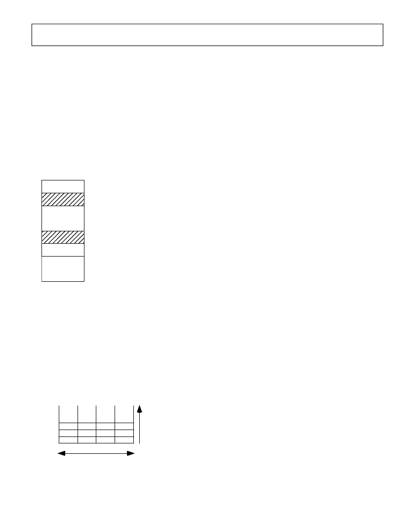
The part incorporates two separate blocks of memory, 8kByte of
SRAM and 64kByte of On-Chip Flash/EE memory. 62kByte of
On-Chip Flash/EE memory are available to the user, and the
remaining 2kBytes are reserved for the factory configured boot
page. These two blocks are mapped as shown in
Figure 4
.
Note that by default, after a reset, the Flash/EE memory is
mirrored at address 0x00000000. It is possible to remap the
SRAM at address 0x00000000 by clearing bit 0 of the REMAP
MMR. This remap function is described in more details in the
Flash/EE memory chapter.
Re-mappable Memory Space
(Flash/EE or SRAM)
Reserved
00080000h
Flash/EE
Reserved
00011FFFh
00010000h
SRAM
FFFF0000h
FFFFFFFFh
MMRs
0000FFFFh
00000000h
0008FFFFh
Figure 4: Physical memory map
Memory Access
The ARM7 core sees memory as a linear array of 232 byte
location where the different blocks of memory are mapped as
outlined in
Figure 4
.
The ADuC702x memory organisation is configured in little
endian format: the least significant byte is located in the lowest
byte address and the most significant byte in the highest byte
address.
Figure 5: little endian format
Flash/EE Memory
The total 64kBytes of Flash/EE are organised as 32k X 16 bits.
31k X 16 bits are user space and 1k X 16 bits is reserved for the
on chip kernel. The page size of this Flash/EE memory is
512Bytes.
62kBytes of Flash/EE are available to the user as code and non-
volatile data memory. There is no distinction between data and
program as ARM code shares the same space. The real width of
the Flash/EE memory is 16 bits, which means that in ARM
mode (32-bit instruction), two accesses to the Flash/EE are
necessary for each instruction fetch. It is therefore
recommended to use Thumb mode when executing from
Flash/EE memory for optimum access speed. The maximum
access speed for the Flash/EE memory is 45MHz in Thumb
mode and 22.5MHz in full ARM mode. More details on
Flash/EE access time are outlined later in ‘Execution from
SRAM and Flash/EE’ section of this datasheet.
SRAM
8kBytes of SRAM are available to the user, organized as 2k X 32
bits, i.e. 2kWords. ARM code can run directly from SRAM at
45MHz , given that the SRAM array is configured as a 32-bit
wide memory array. More details on SRAM access time are
outlined later in ‘Execution from SRAM and Flash/EE’ section
of this datasheet.
Memory Mapped Registers
The Memory Mapped Register (MMR) space is mapped into
the upper 2 pages of the memory array and accessed by indirect
addressing through the ARM7 banked registers.
The MMR space provides an interface between the CPU and all
on-chip peripherals. All registers except the core registers
reside in the MMR area. All shaded locations shown in Figure 6
are unoccupied or reserved locations and should not be
accessed by user software. Table 6 shows a full MMR memory
map.
32 bits
Byte0
Byte1
Byte2
Byte3
0x00000000h
0x00000004h
bit0
bit31
0
1
2
3
4
5
6
7
8
9
A
B
.
.
.
.
0xFFFFFFFFh
相關PDF資料 |
PDF描述 |
|---|---|
| ADUC814ARU-REEL7 | Circular Connector; MIL SPEC:MIL-DTL-38999 Series I; Body Material:Metal; Series:LJT; No. of Contacts:37; Connector Shell Size:25; Connecting Termination:Crimp; Circular Shell Style:Jam Nut Receptacle; Body Style:Straight RoHS Compliant: No |
| ADUC814BRU | Circular Connector; MIL SPEC:MIL-DTL-38999 Series I; Body Material:Metal; Series:LJT; No. of Contacts:37; Connector Shell Size:25; Connecting Termination:Crimp; Circular Shell Style:Jam Nut Receptacle; Body Style:Straight RoHS Compliant: No |
| ADUC814BRU-REEL | Circular Connector; No. of Contacts:56; Series:LJT07R; Body Material:Aluminum; Connecting Termination:Crimp; Connector Shell Size:25; Circular Contact Gender:Pin; Circular Shell Style:Jam Nut Receptacle; Insert Arrangement:25-4 |
| ADUC814BRU-REEL7 | Circular Connector; No. of Contacts:61; Series:LJT07R; Body Material:Aluminum; Connecting Termination:Crimp; Connector Shell Size:25; Circular Contact Gender:Pin; Circular Shell Style:Jam Nut Receptacle; Insert Arrangement:25-61 |
| ADUC814 | MicroConverter, Small Package 12-Bit ADC with Embedded Flash MCU |
相關代理商/技術參數 |
參數描述 |
|---|---|
| ADUC7020 | 制造商:AD 制造商全稱:Analog Devices 功能描述:Precision Analog Microcontroller 12-bit Analog I/O, ARM7TDMI MCU |
| ADUC7020BCP62 | 制造商:Analog Devices 功能描述:FLASH ARM7+5-CH,12-B ADC & 4X12-B DAC IC - Trays |
| ADUC7020BCP62-U1 | 制造商:Analog Devices 功能描述:FLASH ARM7+5-CH,12-B ADC & 4X12-B DAC IC - Trays |
| ADUC7020BCPZ62 | 功能描述:IC MCU FLSH 62K ANLG I/O 40LFCSP RoHS:是 類別:集成電路 (IC) >> 嵌入式 - 微控制器, 系列:MicroConverter® ADuC7xxx 標準包裝:60 系列:PSOC® 3 CY8C38xx 核心處理器:8051 芯體尺寸:8-位 速度:67MHz 連通性:EBI/EMI,I²C,LIN,SPI,UART/USART 外圍設備:電容感應,DMA,LCD,POR,PWM,WDT 輸入/輸出數:25 程序存儲器容量:64KB(64K x 8) 程序存儲器類型:閃存 EEPROM 大小:2K x 8 RAM 容量:8K x 8 電壓 - 電源 (Vcc/Vdd):1.71 V ~ 5.5 V 數據轉換器:A/D 2x20b,D/A 4x8b 振蕩器型:內部 工作溫度:-40°C ~ 85°C 封裝/外殼:48-VFQFN 裸露焊盤 包裝:托盤 |
| ADUC7020BCPZ62I | 功能描述:IC MCU FLSH 62K ANLG I/O 40LFCSP RoHS:是 類別:集成電路 (IC) >> 嵌入式 - 微控制器, 系列:MicroConverter® ADuC7xxx 標準包裝:60 系列:PSOC® 3 CY8C38xx 核心處理器:8051 芯體尺寸:8-位 速度:67MHz 連通性:EBI/EMI,I²C,LIN,SPI,UART/USART 外圍設備:電容感應,DMA,LCD,POR,PWM,WDT 輸入/輸出數:25 程序存儲器容量:64KB(64K x 8) 程序存儲器類型:閃存 EEPROM 大小:2K x 8 RAM 容量:8K x 8 電壓 - 電源 (Vcc/Vdd):1.71 V ~ 5.5 V 數據轉換器:A/D 2x20b,D/A 4x8b 振蕩器型:內部 工作溫度:-40°C ~ 85°C 封裝/外殼:48-VFQFN 裸露焊盤 包裝:托盤 |
發布緊急采購,3分鐘左右您將得到回復。