- 您現在的位置:買賣IC網 > PDF目錄374039 > ADUC702 (Analog Devices, Inc.) 5 AMP MINIATURE POWER RELAY PDF資料下載
參數資料
| 型號: | ADUC702 |
| 廠商: | Analog Devices, Inc. |
| 英文描述: | 5 AMP MINIATURE POWER RELAY |
| 中文描述: | 精密模擬微控制器的12位模擬I / O,ARM7TDMI的微控制器 |
| 文件頁數: | 43/80頁 |
| 文件大小: | 840K |
| 代理商: | ADUC702 |
第1頁第2頁第3頁第4頁第5頁第6頁第7頁第8頁第9頁第10頁第11頁第12頁第13頁第14頁第15頁第16頁第17頁第18頁第19頁第20頁第21頁第22頁第23頁第24頁第25頁第26頁第27頁第28頁第29頁第30頁第31頁第32頁第33頁第34頁第35頁第36頁第37頁第38頁第39頁第40頁第41頁第42頁當前第43頁第44頁第45頁第46頁第47頁第48頁第49頁第50頁第51頁第52頁第53頁第54頁第55頁第56頁第57頁第58頁第59頁第60頁第61頁第62頁第63頁第64頁第65頁第66頁第67頁第68頁第69頁第70頁第71頁第72頁第73頁第74頁第75頁第76頁第77頁第78頁第79頁第80頁
Preliminary Technical Data
ADuC702x Series
high-side or the low-side output. In addition, the Output
Control Unit allows individual enabling/disabling of each of the
six PWM output signals.
Rev. PrB | Page 43 of 80
The Gate Drive Unit permits the generation of the high
frequency chopping frequency and its subsequent mixing with
the PWM signals.
The PWM Shutdown Controller takes care of the PWM
shutdown via the
PWMTRIP
pin and generates the correct
RESET signal for the Timing Unit.
The PWM sync pulse control unit generates the internal
synchronisation pulse and also controls whether the external
SYNC pin is used or not.
The PWM controller is driven by the ADuC702x core clock
frequency and is capable of generating two interrupts to the
ARM core. One interrupt is generated on the occurrence of a
PWMSYNC pulse and the other is generated on the occurrence
of any PWM shutdown action.
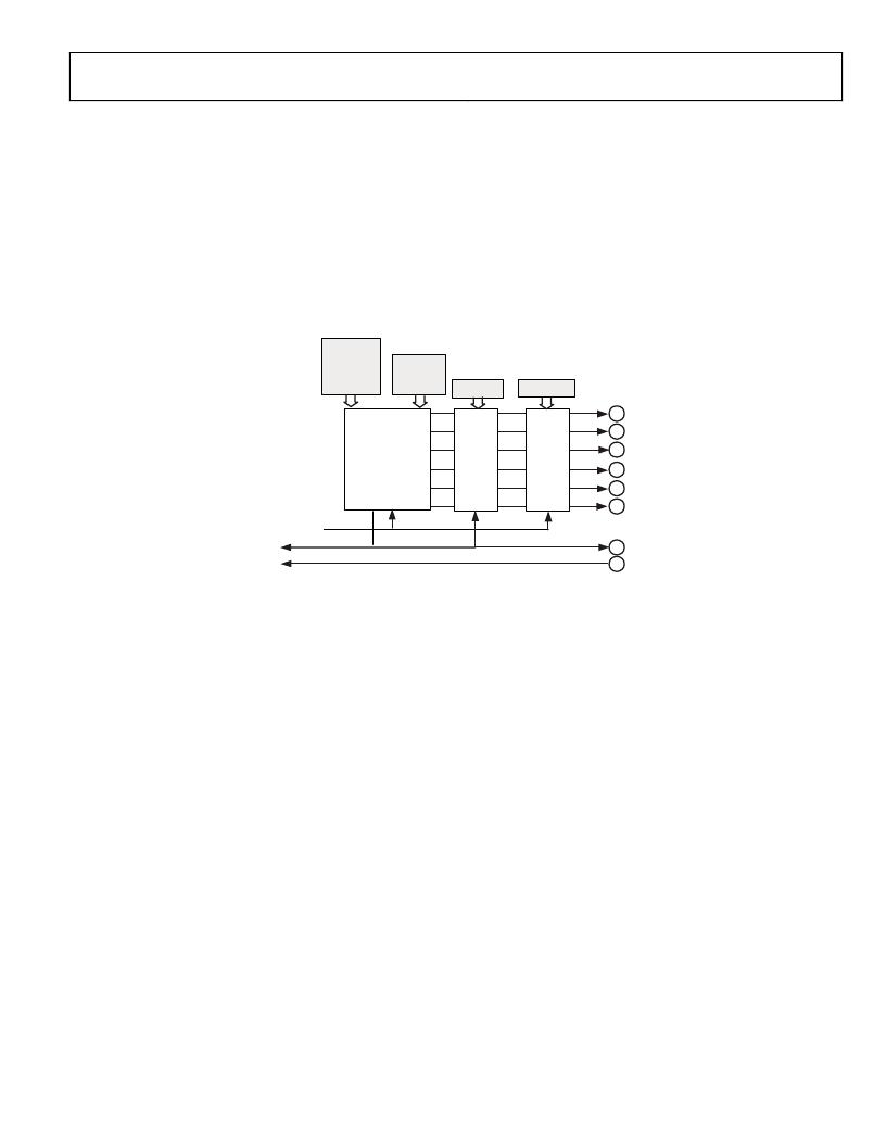
PWMCON
PWMDAT0
PWMDAT1
PWMDAT2
Configuration
Registers
PWMCH0
PWMCH1
PWMCH2
Duty Cycle
Registers
Sync
core clock
PWMEN
PWMCFG
to interrupt
controller
PWM0H
PWM0L
PWM1H
PWM1L
PWM2H
PWM2L
Output
Control
Unit
Gate
Drive
Unit
PWMTRIP
Three-Phase
PWM Timing
Unit
PWMSYNC
Figure 21: Overview of the PWM controller
Three-phase timing unit
PWM Switching Frequency, PWMDAT0 MMR
The PWM switching frequency is controlled by the PWM
period register, PWMDAT0. The fundamental timing unit of
the PWM controller is t
CORE
= 1/f
CORE
where f
CORE
is the core
frequency of the MicroConverter. Therefore, for a 45 MHz
f
CORE
, the fundamental time increment is 21 ns. The value
written to the PWMDAT0 register is effectively the number of
t
CORE
clock increments in half a PWM period. The required
PWMDAT0 value is a function of the desired PWM switching
frequency (f
PWM
) and is given by:
PWMDAT0 = f
core
/ (2 x f
PWM
)
Therefore, the PWM switching period, Ts, can be written as:
Ts = 2 x PWMDAT0 x t
CORE
The largest value that can be written to the 16-bit PWMDAT0
MMR is 0xFFFF = 65535 which corresponds to a minimum
PWM switching frequency of:
f
PWM(min)
= 45 x 10
6
/ (2 x 65535) = 343.99 Hz
Note that PWMDAT0 value of 0 and 1 are not defined and
should not be used.
PWM Switching Dead Time, PWMDAT1 MMR
The second important parameter that must be set up in the
initial configuration of the PWM block is the switching dead
time. This is a short delay time introduced between turning off
one PWM signal (e.g. AH) and turning on the complementary
signal (AL). This short time delay is introduced to permit the
power switch being turned off (in this case, AH) to completely
recover its blocking capability before the complementary switch
is turned on. This time delay prevents a potentially destructive
short-circuit condition from developing across the dc link
capacitor of a typical voltage source inverter.
The dead time is controlled by the 10-bit, read/write
PWMDAT1 register. There is only one dead-time register that
controls the dead time inserted into all three pairs of PWM
output signals. The dead time, TD, is related to the value in the
PWMDAT1 register by:
TD = PWMDAT1 × 2 × t
CORE
Therefore, a PWMDAT1 value of 0x00A (= 10), introduces an
426 ns delay between the turn-off on any PWM signal (say, AH)
and the turn-on of its complementary signal (AL). The amount
相關PDF資料 |
PDF描述 |
|---|---|
| ADUC814ARU-REEL7 | Circular Connector; MIL SPEC:MIL-DTL-38999 Series I; Body Material:Metal; Series:LJT; No. of Contacts:37; Connector Shell Size:25; Connecting Termination:Crimp; Circular Shell Style:Jam Nut Receptacle; Body Style:Straight RoHS Compliant: No |
| ADUC814BRU | Circular Connector; MIL SPEC:MIL-DTL-38999 Series I; Body Material:Metal; Series:LJT; No. of Contacts:37; Connector Shell Size:25; Connecting Termination:Crimp; Circular Shell Style:Jam Nut Receptacle; Body Style:Straight RoHS Compliant: No |
| ADUC814BRU-REEL | Circular Connector; No. of Contacts:56; Series:LJT07R; Body Material:Aluminum; Connecting Termination:Crimp; Connector Shell Size:25; Circular Contact Gender:Pin; Circular Shell Style:Jam Nut Receptacle; Insert Arrangement:25-4 |
| ADUC814BRU-REEL7 | Circular Connector; No. of Contacts:61; Series:LJT07R; Body Material:Aluminum; Connecting Termination:Crimp; Connector Shell Size:25; Circular Contact Gender:Pin; Circular Shell Style:Jam Nut Receptacle; Insert Arrangement:25-61 |
| ADUC814 | MicroConverter, Small Package 12-Bit ADC with Embedded Flash MCU |
相關代理商/技術參數 |
參數描述 |
|---|---|
| ADUC7020 | 制造商:AD 制造商全稱:Analog Devices 功能描述:Precision Analog Microcontroller 12-bit Analog I/O, ARM7TDMI MCU |
| ADUC7020BCP62 | 制造商:Analog Devices 功能描述:FLASH ARM7+5-CH,12-B ADC & 4X12-B DAC IC - Trays |
| ADUC7020BCP62-U1 | 制造商:Analog Devices 功能描述:FLASH ARM7+5-CH,12-B ADC & 4X12-B DAC IC - Trays |
| ADUC7020BCPZ62 | 功能描述:IC MCU FLSH 62K ANLG I/O 40LFCSP RoHS:是 類別:集成電路 (IC) >> 嵌入式 - 微控制器, 系列:MicroConverter® ADuC7xxx 標準包裝:60 系列:PSOC® 3 CY8C38xx 核心處理器:8051 芯體尺寸:8-位 速度:67MHz 連通性:EBI/EMI,I²C,LIN,SPI,UART/USART 外圍設備:電容感應,DMA,LCD,POR,PWM,WDT 輸入/輸出數:25 程序存儲器容量:64KB(64K x 8) 程序存儲器類型:閃存 EEPROM 大小:2K x 8 RAM 容量:8K x 8 電壓 - 電源 (Vcc/Vdd):1.71 V ~ 5.5 V 數據轉換器:A/D 2x20b,D/A 4x8b 振蕩器型:內部 工作溫度:-40°C ~ 85°C 封裝/外殼:48-VFQFN 裸露焊盤 包裝:托盤 |
| ADUC7020BCPZ62I | 功能描述:IC MCU FLSH 62K ANLG I/O 40LFCSP RoHS:是 類別:集成電路 (IC) >> 嵌入式 - 微控制器, 系列:MicroConverter® ADuC7xxx 標準包裝:60 系列:PSOC® 3 CY8C38xx 核心處理器:8051 芯體尺寸:8-位 速度:67MHz 連通性:EBI/EMI,I²C,LIN,SPI,UART/USART 外圍設備:電容感應,DMA,LCD,POR,PWM,WDT 輸入/輸出數:25 程序存儲器容量:64KB(64K x 8) 程序存儲器類型:閃存 EEPROM 大小:2K x 8 RAM 容量:8K x 8 電壓 - 電源 (Vcc/Vdd):1.71 V ~ 5.5 V 數據轉換器:A/D 2x20b,D/A 4x8b 振蕩器型:內部 工作溫度:-40°C ~ 85°C 封裝/外殼:48-VFQFN 裸露焊盤 包裝:托盤 |
發布緊急采購,3分鐘左右您將得到回復。