- 您現(xiàn)在的位置:買賣IC網(wǎng) > PDF目錄374039 > ADUC702 (Analog Devices, Inc.) 5 AMP MINIATURE POWER RELAY PDF資料下載
參數(shù)資料
| 型號(hào): | ADUC702 |
| 廠商: | Analog Devices, Inc. |
| 英文描述: | 5 AMP MINIATURE POWER RELAY |
| 中文描述: | 精密模擬微控制器的12位模擬I / O,ARM7TDMI的微控制器 |
| 文件頁數(shù): | 76/80頁 |
| 文件大小: | 840K |
| 代理商: | ADUC702 |
第1頁第2頁第3頁第4頁第5頁第6頁第7頁第8頁第9頁第10頁第11頁第12頁第13頁第14頁第15頁第16頁第17頁第18頁第19頁第20頁第21頁第22頁第23頁第24頁第25頁第26頁第27頁第28頁第29頁第30頁第31頁第32頁第33頁第34頁第35頁第36頁第37頁第38頁第39頁第40頁第41頁第42頁第43頁第44頁第45頁第46頁第47頁第48頁第49頁第50頁第51頁第52頁第53頁第54頁第55頁第56頁第57頁第58頁第59頁第60頁第61頁第62頁第63頁第64頁第65頁第66頁第67頁第68頁第69頁第70頁第71頁第72頁第73頁第74頁第75頁當(dāng)前第76頁第77頁第78頁第79頁第80頁
ADuC702x Series
Preliminary Technical Data
digital and analog sections, as illustrated in Figure 41c.
Rev. PrB | Page 76 of 80
b.
DGND
AGND
PLACE ANALOG
COMPONENTS
HERE
PLACE DIGITAL
COMPONENTS
HERE
c.
GND
PLACE ANALOG
COMPONENTS
HERE
PLACE DIGITAL
COMPONENTS
HERE
DGND
PLACE ANALOG
COMPONENTS HERE
a.
AGND
PLACE DIGITAL
COMPONENTS HERE
Figure 41:. System grounding schemes
In all of these scenarios, and in more complicated real-life
applications, keep in mind the flow of current from the supplies
and back to ground. Make sure the return paths for all currents
are as close as possible to the paths the currents took to reach
their destinations. For example, do not power components on
the analog side of Figure 41b with IOV
DD
since that would force
return currents from IOV
DD
to flow through AGND. Also, try
to avoid digital currents flowing under analog circuitry, which
could happen if the user placed a noisy digital chip on the left
half of the board in Figure 41c. Whenever possible, avoid large
discontinuities in the ground plane(s) (such as are formed by a
long trace on the same layer), since they force return signals to
travel a longer path. And of course, make all connections to the
ground plane directly, with little or no trace separating the pin
from its via to ground.
If the user plans to connect fast logic signals (rise/fall time < 5
ns) to any of the ADuC702x’s digital inputs, add a series
resistor to each relevant line to keep rise and fall times longer
than 5 ns at the ADuC702x input pins. A value of 100
or
200
is usually sufficient to prevent high speed signals from
coupling capacitively into the ADuC702x and affecting the
accuracy of ADC conversions.
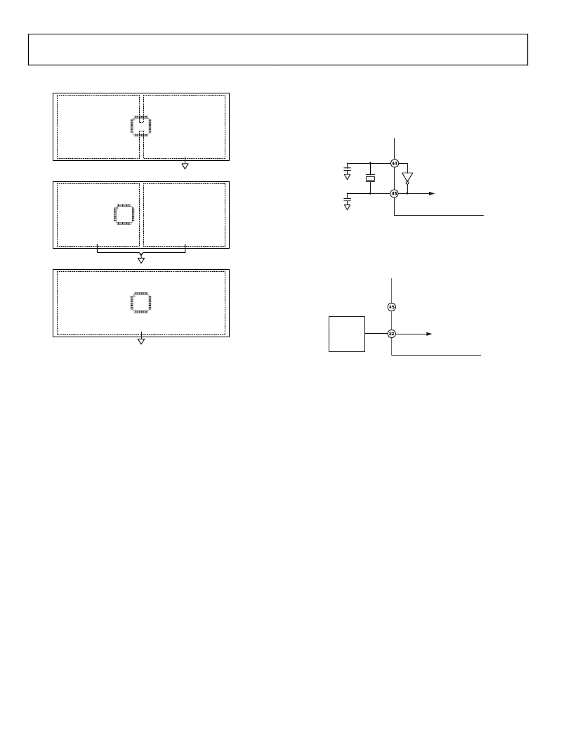
CLOCK OSCILLATOR
The clock source for the ADuC702x can be generated by the
internal PLL or by an external clock input. To use the internal
PLL, connect a 32.768kHz parallel resonant crystal between
XCLKI and XCLKO and connect a capacitor from each pin to
ground as shown Figure 42 This crystal allows the PLL to lock
correctly to give a frequency of 45.088MHz. If no external
crystal is present, the internal oscillator will be used to give a
frequency of 45.088MHz
±
5% typically.
12pF
XCLKI
XCLKO
32.768kHz
TO INTERNAL
PLL
ADuC7026
12pF
Figure 42: external parallel resonant crystal connections
To use an external source clock input instead of the PLL, bit 1
and bit 0 of PLLCON must be modified. The external clock
uses pin 17, XCLK.
TO FREQUENCY
DIVIDER
ADuC7026
XCLK
EXTERNAL
CLOCK
SOURCE
XCLKI
Figure 43:connecting an external clock source
Whether using the internal PLL or an external clock source, the
ADuC702x’s specified operational clock speed range is 50kHz
to 20MHz to ensure correct operation of the analog peripherals
and Flash/EE.
POWER-ON RESET OPERATION
An internal POR (Power-On Reset) is implemented on the
ADuC702x. For LV
DD
below 1.98 V, the internal POR will hold
the ADuC702x in reset. As LV
DD
rises above 1.98 V, an internal
timer will time out for typically 128 ms before the part is
released from reset. The user must ensure that the power
supply IOV
DD
has reached a stable 2.7 V minimum level by this
time. Likewise on power-down, the internal POR will hold the
ADuC702x in reset until LV
DD
has dropped below 1.98V.
Figure 44 illustrates the operation of the internal POR in detail.
相關(guān)PDF資料 |
PDF描述 |
|---|---|
| ADUC814ARU-REEL7 | Circular Connector; MIL SPEC:MIL-DTL-38999 Series I; Body Material:Metal; Series:LJT; No. of Contacts:37; Connector Shell Size:25; Connecting Termination:Crimp; Circular Shell Style:Jam Nut Receptacle; Body Style:Straight RoHS Compliant: No |
| ADUC814BRU | Circular Connector; MIL SPEC:MIL-DTL-38999 Series I; Body Material:Metal; Series:LJT; No. of Contacts:37; Connector Shell Size:25; Connecting Termination:Crimp; Circular Shell Style:Jam Nut Receptacle; Body Style:Straight RoHS Compliant: No |
| ADUC814BRU-REEL | Circular Connector; No. of Contacts:56; Series:LJT07R; Body Material:Aluminum; Connecting Termination:Crimp; Connector Shell Size:25; Circular Contact Gender:Pin; Circular Shell Style:Jam Nut Receptacle; Insert Arrangement:25-4 |
| ADUC814BRU-REEL7 | Circular Connector; No. of Contacts:61; Series:LJT07R; Body Material:Aluminum; Connecting Termination:Crimp; Connector Shell Size:25; Circular Contact Gender:Pin; Circular Shell Style:Jam Nut Receptacle; Insert Arrangement:25-61 |
| ADUC814 | MicroConverter, Small Package 12-Bit ADC with Embedded Flash MCU |
相關(guān)代理商/技術(shù)參數(shù) |
參數(shù)描述 |
|---|---|
| ADUC7020 | 制造商:AD 制造商全稱:Analog Devices 功能描述:Precision Analog Microcontroller 12-bit Analog I/O, ARM7TDMI MCU |
| ADUC7020BCP62 | 制造商:Analog Devices 功能描述:FLASH ARM7+5-CH,12-B ADC & 4X12-B DAC IC - Trays |
| ADUC7020BCP62-U1 | 制造商:Analog Devices 功能描述:FLASH ARM7+5-CH,12-B ADC & 4X12-B DAC IC - Trays |
| ADUC7020BCPZ62 | 功能描述:IC MCU FLSH 62K ANLG I/O 40LFCSP RoHS:是 類別:集成電路 (IC) >> 嵌入式 - 微控制器, 系列:MicroConverter® ADuC7xxx 標(biāo)準(zhǔn)包裝:60 系列:PSOC® 3 CY8C38xx 核心處理器:8051 芯體尺寸:8-位 速度:67MHz 連通性:EBI/EMI,I²C,LIN,SPI,UART/USART 外圍設(shè)備:電容感應(yīng),DMA,LCD,POR,PWM,WDT 輸入/輸出數(shù):25 程序存儲(chǔ)器容量:64KB(64K x 8) 程序存儲(chǔ)器類型:閃存 EEPROM 大小:2K x 8 RAM 容量:8K x 8 電壓 - 電源 (Vcc/Vdd):1.71 V ~ 5.5 V 數(shù)據(jù)轉(zhuǎn)換器:A/D 2x20b,D/A 4x8b 振蕩器型:內(nèi)部 工作溫度:-40°C ~ 85°C 封裝/外殼:48-VFQFN 裸露焊盤 包裝:托盤 |
| ADUC7020BCPZ62I | 功能描述:IC MCU FLSH 62K ANLG I/O 40LFCSP RoHS:是 類別:集成電路 (IC) >> 嵌入式 - 微控制器, 系列:MicroConverter® ADuC7xxx 標(biāo)準(zhǔn)包裝:60 系列:PSOC® 3 CY8C38xx 核心處理器:8051 芯體尺寸:8-位 速度:67MHz 連通性:EBI/EMI,I²C,LIN,SPI,UART/USART 外圍設(shè)備:電容感應(yīng),DMA,LCD,POR,PWM,WDT 輸入/輸出數(shù):25 程序存儲(chǔ)器容量:64KB(64K x 8) 程序存儲(chǔ)器類型:閃存 EEPROM 大小:2K x 8 RAM 容量:8K x 8 電壓 - 電源 (Vcc/Vdd):1.71 V ~ 5.5 V 數(shù)據(jù)轉(zhuǎn)換器:A/D 2x20b,D/A 4x8b 振蕩器型:內(nèi)部 工作溫度:-40°C ~ 85°C 封裝/外殼:48-VFQFN 裸露焊盤 包裝:托盤 |
發(fā)布緊急采購,3分鐘左右您將得到回復(fù)。