- 您現在的位置:買賣IC網 > PDF目錄374039 > ADUC814 (Analog Devices, Inc.) MicroConverter, Small Package 12-Bit ADC with Embedded Flash MCU PDF資料下載
參數資料
| 型號: | ADUC814 |
| 廠商: | Analog Devices, Inc. |
| 英文描述: | MicroConverter, Small Package 12-Bit ADC with Embedded Flash MCU |
| 中文描述: | MicroConverter的,小包裝12位ADC,嵌入式閃存MCU |
| 文件頁數: | 10/72頁 |
| 文件大小: | 846K |
| 代理商: | ADUC814 |
第1頁第2頁第3頁第4頁第5頁第6頁第7頁第8頁第9頁當前第10頁第11頁第12頁第13頁第14頁第15頁第16頁第17頁第18頁第19頁第20頁第21頁第22頁第23頁第24頁第25頁第26頁第27頁第28頁第29頁第30頁第31頁第32頁第33頁第34頁第35頁第36頁第37頁第38頁第39頁第40頁第41頁第42頁第43頁第44頁第45頁第46頁第47頁第48頁第49頁第50頁第51頁第52頁第53頁第54頁第55頁第56頁第57頁第58頁第59頁第60頁第61頁第62頁第63頁第64頁第65頁第66頁第67頁第68頁第69頁第70頁第71頁第72頁
ADuC814
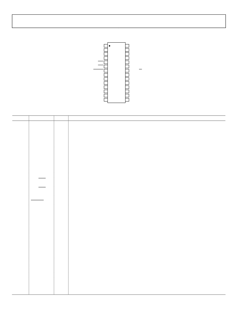
PIN CONFIGURATION AND FUNCTION DESCRIPTION
Rev. A | Page 10 of 72
ADuC814
TOP VIEW
(Not to Scale)
DGND
1
DLOAD
2
P3.0/RxD
3
P3.1/TxD
4
P3.2/INT0
5
DV
DD
XTAL2
XTAL1
SCLOCK
P3.7/SDATA/MOSI
28
27
26
25
24
P3.3/INT1
6
P3.4/T0/CONVST
7
P1.0/T2
8
P1.1/T2EX
9
P3.6/MISO
P3.5/T1/SS/EXTCLK
P1.7/ADC5/DAC1
P1.6/ADC4/DAC0
23
22
21
20
RESET
10
P1.5/ADC3
19
P1.2/ADC0
11
P1.3/ADC1
12
AV
DD
AGND
14
13
P1.4/ADC2
C
REF
V
REF
AGND
18
17
16
15
0
Figure 2. Pin Configuration
Table 3. Pin Descriptions
Pin No.
Mnemonic
1
DGND
2
DLOAD
Type
S
I
Function
Digital Ground. Ground reference point for the digital circuitry.
Debug/Serial Download Mode. Enables when pulled high through a resistor on power-on or RESET. In
this mode, DLOAD may also be used as an external emulation I/O pin, therefore the voltage level at
this pin must not be changed during this mode of operation because it may cause an emulation
interrupt that halts code execution. User code is executed when this pin is pulled low on power-on or
RESET.
Bidirectional Port Pins with Internal Pull-Up Resistors. Port 3 pins that have 1s written to them are
pulled high by the internal pull-up resistors, and in that state they can be used as inputs. As inputs,
with Port 3 pins being pulled low externally, they source current because of the internal pull-up
resistors. When driving a 0-to-1 output transition, a strong pull-up is active during S1 of the
instruction cycle. Port 3 pins also have various secondary functions which are described next.
Receiver Data Input (asynchronous) or Data Input/Output (synchronous) in Serial (UART) Mode.
Transmitter Data Output (asynchronous) or Clock Output (synchronous) in Serial (UART) Mode.
Interrupt 0, programmable edge or level-triggered interrupt input, which can be programmed to one
of two priority levels. This pin can also be used as agate control input to Timer 0.
Interrupt 1, programmable edge or level-triggered interrupt input, which can be programmed to one
of two priority levels. This pin can also be used as agate control input to Timer 1.
Timer/Counter 0 Input and External Trigger Input for ADC Conversion Start.
3–7
P3.0 – P3.4
I/O
3
4
5
P3.0/RxD
P3.1/TxD
P3.2/INT0
I/O
I/O
I/O
6
P3.3/INT1
I/O
7
P3.4/T0/
CONVST
P1.0–P1.1
I/O
8–9
I/O
Bidirectional Port Pins with Internal Pull-Up Resistors. Port 1 pins that have 1s written to them are
pulled high by the internal pull-up resistors, and in that state they can be used as inputs. As inputs
,with Port 1 pins being pulled low externally, they source current because of the internal pull-up
resistors When driving a 0-to-1 output transition a strong pull-up is active during S1 of the instruction
cycle. Port 1 pins also have various secondary functions which are described as follows.
Timer 2 Digital Input. Input to Timer/Counter 2. When enabled, Counter 2 is incremented in response
to a 1 to 0 transition of the T2 input.
Digital Input. Capture/Reload trigger for Counter 2.
Reset Input. A high level on this pin while the oscillator is running resets the device. There is an
internal weak pull-down and a Schmitt-trigger input stage on this pin.
Port 1.2 to P1.3. These pins have no digital output drivers, i.e., they can only function as digital inputs,
for which 0 must be written to the port bit. These port pins also have the following analog functionality:
ADC Input Channel 0. Selected via ADCCON2 SFR.
ADC Input Channel 1. Selected via ADCCON2 SFR.
Analog Positive Supply Voltage, 3 V or 5 V.
Analog Ground. Ground reference point for the analog circuitry.
Reference Input/Output. This pin is connected to the internal reference through a switch and is the
reference source for the analog to digital converter. The nominal internal reference voltage is 2.5 V
and this appears at the pin. This pin can be used to connect an external reference to the analog to
digital converter by setting ADCCON1.6 to 1. Connect 0.1 μF between this pin and AGND.
8
P1.0/T2
I/O
9
10
P1.1/T2EX
RESET
I/O
I
11–12
P1.2–P1.3
I
11
12
13
14–15
16
P1.2/ADC0
P1.3/ADC1
AV
DD
AGND
V
REF
I
I
S
G
I/O
相關PDF資料 |
PDF描述 |
|---|---|
| ADUC814ARU | MicroConverter, Small Package 12-Bit ADC with Embedded Flash MCU |
| ADUC814ARU-REEL | MicroConverter, Small Package 12-Bit ADC with Embedded Flash MCU |
| ADUC824 | MicroConverter, Dual-Channel 16-/24-Bit ADCs with Embedded FLASH MCU |
| ADUC824BS | MicroConverter, Dual-Channel 16-/24-Bit ADCs with Embedded FLASH MCU |
| ADUC831 | LJT 6C 6#22D PIN RECP |
相關代理商/技術參數 |
參數描述 |
|---|---|
| ADUC814_02 | 制造商:AD 制造商全稱:Analog Devices 功能描述:MicroConverter, Small Package 12-Bit ADC with Embedded FLASH MCU |
| ADUC814AN | 功能描述:8052 MicroConverter? ADuC8xx Microcontroller IC 8-Bit 16.78MHz 8KB (8K x 8) FLASH 制造商:analog devices inc. 系列:MicroConverter? ADuC8xx 包裝:- 零件狀態:上次購買時間 核心處理器:8052 核心尺寸:8-位 速度:16.78MHz 連接性:I2C,SPI,UART/USART 外設:POR,PSM,溫度傳感器,WDT I/O 數:- 程序存儲容量:8KB(8K x 8) 程序存儲器類型:閃存 EEPROM 容量:640 x 8 RAM 容量:256 x 8 電壓 - 電源(Vcc/Vdd):2.7 V ~ 5.5 V 數據轉換器:* 振蕩器類型:內部 工作溫度:* 封裝/外殼:- 供應商器件封裝:- 標準包裝:1 |
| ADUC814ARU | 功能描述:IC ADC 12BIT W/FLASH MCU 28TSSOP RoHS:否 類別:集成電路 (IC) >> 嵌入式 - 微控制器, 系列:MicroConverter® ADuC8xx 標準包裝:38 系列:Encore!® XP® 核心處理器:eZ8 芯體尺寸:8-位 速度:5MHz 連通性:IrDA,UART/USART 外圍設備:欠壓檢測/復位,LED,POR,PWM,WDT 輸入/輸出數:16 程序存儲器容量:4KB(4K x 8) 程序存儲器類型:閃存 EEPROM 大小:- RAM 容量:1K x 8 電壓 - 電源 (Vcc/Vdd):2.7 V ~ 3.6 V 數據轉換器:- 振蕩器型:內部 工作溫度:-40°C ~ 105°C 封裝/外殼:20-SOIC(0.295",7.50mm 寬) 包裝:管件 其它名稱:269-4116Z8F0413SH005EG-ND |
| ADUC814ARU-D2 | 制造商:Analog Devices 功能描述:12 BIT ADC WITH EMBEDDED 8-BIT MICRO I.C - Tape and Reel 制造商:Rochester Electronics LLC 功能描述:12 BIT ADC WITH EMBEDDED 8-BIT MICRO I.C - Bulk |
| ADUC814ARU-REEL | 制造商:Analog Devices 功能描述:MCU 8-Bit ADuC8xx 8052 CISC 8KB Flash 3V/5V 28-Pin TSSOP T/R 制造商:Analog Devices 功能描述:12 BIT ADC WITH EMBEDDED 8-BIT MICRO I.C - Tape and Reel |
發布緊急采購,3分鐘左右您將得到回復。