- 您現在的位置:買賣IC網 > PDF目錄374039 > ADUC814 (Analog Devices, Inc.) MicroConverter, Small Package 12-Bit ADC with Embedded Flash MCU PDF資料下載
參數資料
| 型號: | ADUC814 |
| 廠商: | Analog Devices, Inc. |
| 英文描述: | MicroConverter, Small Package 12-Bit ADC with Embedded Flash MCU |
| 中文描述: | MicroConverter的,小包裝12位ADC,嵌入式閃存MCU |
| 文件頁數: | 35/72頁 |
| 文件大小: | 846K |
| 代理商: | ADUC814 |
第1頁第2頁第3頁第4頁第5頁第6頁第7頁第8頁第9頁第10頁第11頁第12頁第13頁第14頁第15頁第16頁第17頁第18頁第19頁第20頁第21頁第22頁第23頁第24頁第25頁第26頁第27頁第28頁第29頁第30頁第31頁第32頁第33頁第34頁當前第35頁第36頁第37頁第38頁第39頁第40頁第41頁第42頁第43頁第44頁第45頁第46頁第47頁第48頁第49頁第50頁第51頁第52頁第53頁第54頁第55頁第56頁第57頁第58頁第59頁第60頁第61頁第62頁第63頁第64頁第65頁第66頁第67頁第68頁第69頁第70頁第71頁第72頁
ADuC814
DACxH/L
Function
SFR Address
Power-On Default
Bit Addressable
Rev. A | Page 35 of 72
DAC0 and DAC1 Data Registers
DAC Data Registers, written by the user to update the DAC outputs.
DAC0L (DAC0 data low byte) –> F9H DAC0H (DAC0 data high byte) –> FAH;
DAC1L (DAC1 data low byte) –> FBH DAC1H (DAC1 data high byte) –> FCH
00H –> Both DAC0 and DAC1 data registers.
No –> Both DAC0 and DAC1 data registers.
The 12-bit DAC data should be written into DACxH/L right-justified such that DACL contains the lower eight bits, and the lower nibble
of DACH contains the upper four bits.
Using the DACs
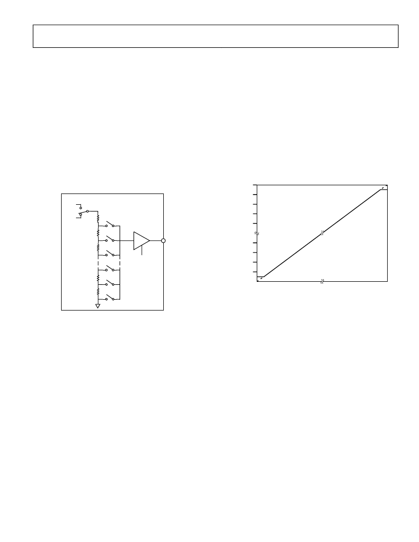
The on-chip DAC architecture consists of a resistor string DAC
followed by an output buffer amplifier, the functional equivalent
of which is illustrated in Figure 38. Features of this architecture
include inherent guaranteed monotonicity and excellent differ-
ential linearity.
OUTPUT
BUFFER
HIGH Z
DISABLE
(FROM MCU)
DAC0
R
R
R
R
R
ADuC814
AV
DD
V
REF
0
Figure 38. Resistor String DAC Functional Equivalent
As illustrated in Figure 38, the reference source for each DAC is
user selectable in software. It can be either AV
DD
or V
REF
. In
0 V-to-AV
DD
mode, the DAC output transfer function spans
from 0 V to the voltage at the AV
DD
pin. In 0 V-to-V
REF
mode,
the DAC output transfer function spans from 0 V to the internal
V
REF
, or if an external reference is applied, the voltage at the V
REF
pin. The DAC output buffer features a true rail-to-rail output
stage implementation. This means that, unloaded, each output is
capable of swinging to within less than 100 mV of both AV
DD
and ground. Moreover, the DAC’s linearity specification (when
driving a 10 k resistive load to ground) is guaranteed through
the full transfer function except Codes 0 to 48, and, in 0 V-to-
AV
DD
mode only, Codes 3945 to 4095. Linearity degradation
near ground and V
DD
is caused by saturation of the output
buffer, and a general representation of its effects (neglecting
offset and gain error) is illustrated in Figure 39. The dotted line
in Figure 39 indicates the ideal transfer function, and the solid
line represents what the transfer function might look like with
endpoint nonlinearities due to saturation of the output buffer.
Note that Figure 39 represents a transfer function in 0 V-to-V
DD
mode only. In 0 V-to-V
REF
mode (with V
REF
< V
DD
), the lower
nonlinearity would be similar, but the upper portion of the
transfer function would follow the ideal line right to the end
(V
REF
in this case, not V
DD
), showing no signs of upper endpoint
linearity error.
V
DD
V
DD
–50mV
50mV
0mV
V
DD
–100mV
100mV
000H
FFFH
0
Figure 39. Endpoint Nonlinearities Due to Amplifier Saturation
The endpoint nonlinearities conceptually illustrated in Figure 39
get worse as a function of output loading. Most ADuC814
specifications assume a 10 k resistive load to ground at the
DAC output. As the output is forced to source or sink more
current, the nonlinear regions at the top or bottom (respectively)
of Figure 39 become larger. With larger current demands, this
can significantly limit output voltage swing. Figure 40 and
Figure 41 illustrate this behavior. Note that the upper trace in
each of these figures is valid only for an output range selection
of 0 V-to-AV
DD
. In 0 V-to-V
REF
mode, DAC loading does not
cause high-side voltage drops as long as the reference voltage
remains below the upper trace in the corresponding figure. For
example, if AV
DD
= 3 V and V
REF
= 2.5 V, the high-side voltage is
not affected by loads less than 5 mA. But around 7 mA, the
upper curve in Figure 41 drops below 2.5 V (V
REF
), indicating
that at these higher currents the output cannot reach V
REF
.
相關PDF資料 |
PDF描述 |
|---|---|
| ADUC814ARU | MicroConverter, Small Package 12-Bit ADC with Embedded Flash MCU |
| ADUC814ARU-REEL | MicroConverter, Small Package 12-Bit ADC with Embedded Flash MCU |
| ADUC824 | MicroConverter, Dual-Channel 16-/24-Bit ADCs with Embedded FLASH MCU |
| ADUC824BS | MicroConverter, Dual-Channel 16-/24-Bit ADCs with Embedded FLASH MCU |
| ADUC831 | LJT 6C 6#22D PIN RECP |
相關代理商/技術參數 |
參數描述 |
|---|---|
| ADUC814_02 | 制造商:AD 制造商全稱:Analog Devices 功能描述:MicroConverter, Small Package 12-Bit ADC with Embedded FLASH MCU |
| ADUC814AN | 功能描述:8052 MicroConverter? ADuC8xx Microcontroller IC 8-Bit 16.78MHz 8KB (8K x 8) FLASH 制造商:analog devices inc. 系列:MicroConverter? ADuC8xx 包裝:- 零件狀態:上次購買時間 核心處理器:8052 核心尺寸:8-位 速度:16.78MHz 連接性:I2C,SPI,UART/USART 外設:POR,PSM,溫度傳感器,WDT I/O 數:- 程序存儲容量:8KB(8K x 8) 程序存儲器類型:閃存 EEPROM 容量:640 x 8 RAM 容量:256 x 8 電壓 - 電源(Vcc/Vdd):2.7 V ~ 5.5 V 數據轉換器:* 振蕩器類型:內部 工作溫度:* 封裝/外殼:- 供應商器件封裝:- 標準包裝:1 |
| ADUC814ARU | 功能描述:IC ADC 12BIT W/FLASH MCU 28TSSOP RoHS:否 類別:集成電路 (IC) >> 嵌入式 - 微控制器, 系列:MicroConverter® ADuC8xx 標準包裝:38 系列:Encore!® XP® 核心處理器:eZ8 芯體尺寸:8-位 速度:5MHz 連通性:IrDA,UART/USART 外圍設備:欠壓檢測/復位,LED,POR,PWM,WDT 輸入/輸出數:16 程序存儲器容量:4KB(4K x 8) 程序存儲器類型:閃存 EEPROM 大小:- RAM 容量:1K x 8 電壓 - 電源 (Vcc/Vdd):2.7 V ~ 3.6 V 數據轉換器:- 振蕩器型:內部 工作溫度:-40°C ~ 105°C 封裝/外殼:20-SOIC(0.295",7.50mm 寬) 包裝:管件 其它名稱:269-4116Z8F0413SH005EG-ND |
| ADUC814ARU-D2 | 制造商:Analog Devices 功能描述:12 BIT ADC WITH EMBEDDED 8-BIT MICRO I.C - Tape and Reel 制造商:Rochester Electronics LLC 功能描述:12 BIT ADC WITH EMBEDDED 8-BIT MICRO I.C - Bulk |
| ADUC814ARU-REEL | 制造商:Analog Devices 功能描述:MCU 8-Bit ADuC8xx 8052 CISC 8KB Flash 3V/5V 28-Pin TSSOP T/R 制造商:Analog Devices 功能描述:12 BIT ADC WITH EMBEDDED 8-BIT MICRO I.C - Tape and Reel |
發布緊急采購,3分鐘左右您將得到回復。