- 您現在的位置:買賣IC網 > PDF目錄374044 > ADV601 (Analog Devices, Inc.) Low Cost Multiformat Video Codec PDF資料下載
參數資料
| 型號: | ADV601 |
| 廠商: | Analog Devices, Inc. |
| 元件分類: | 視頻Codec |
| 英文描述: | Low Cost Multiformat Video Codec |
| 中文描述: | 低成本多格式視頻解碼器 |
| 文件頁數: | 43/52頁 |
| 文件大小: | 606K |
| 代理商: | ADV601 |
第1頁第2頁第3頁第4頁第5頁第6頁第7頁第8頁第9頁第10頁第11頁第12頁第13頁第14頁第15頁第16頁第17頁第18頁第19頁第20頁第21頁第22頁第23頁第24頁第25頁第26頁第27頁第28頁第29頁第30頁第31頁第32頁第33頁第34頁第35頁第36頁第37頁第38頁第39頁第40頁第41頁第42頁當前第43頁第44頁第45頁第46頁第47頁第48頁第49頁第50頁第51頁第52頁
ADV601
–43–
REV. 0
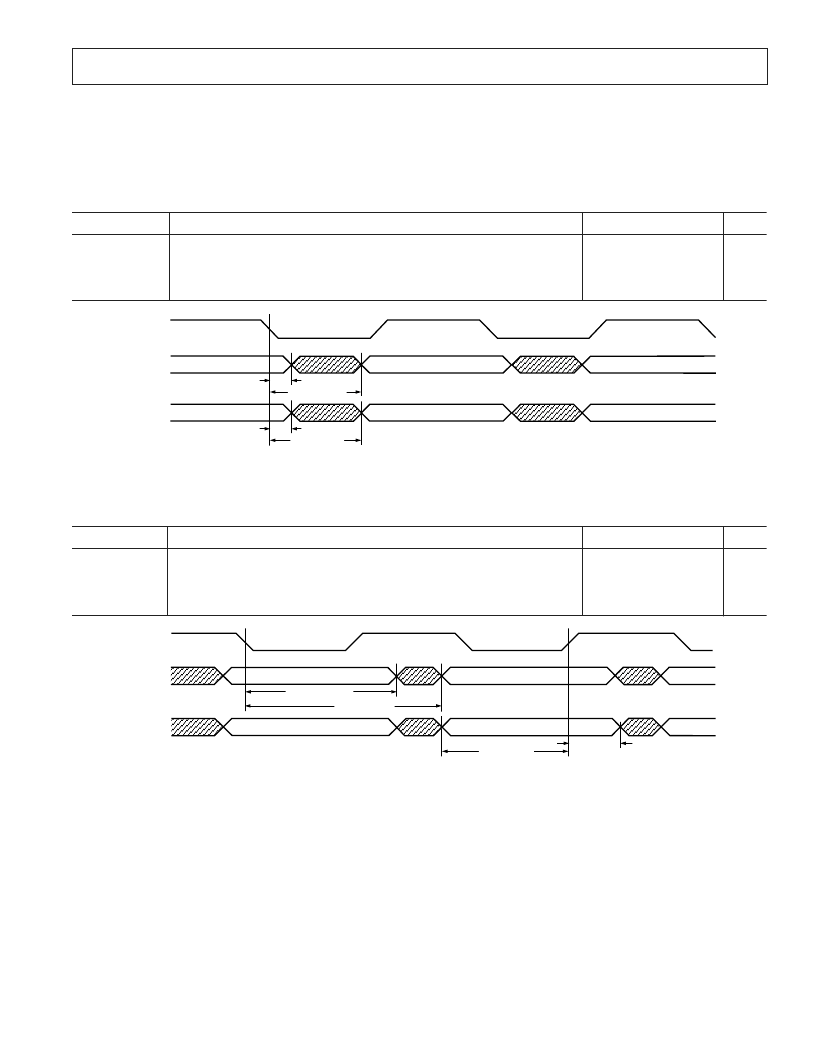
Multiplexed Philips Video Timing
The diagrams in this section show transfer timing for pixel (YCrCb) data in Multiplexed Philips video mode. For line (horizontal)
and frame (vertical) data transfer timing, see the Gray Scale/Philips Video Timing section. All output values assume a maximum pin
loading of 50 pF. Note that in timing diagrams for Multiplexed Philips video, the label CTRL indicates the VSYNC, HSYNC and
FIELD pins. Also note that for Multiplexed Philips mode the CREF pin is unused.
Table XXIX. Multiplexed Philips Video—Decode and Master Pixel (YCrCb) Timing Parameters
Parameter
Description
Min
Max
Unit
t
VDATA_DMM_D
t
VDATA_DMM_OH
t
CTRL_DMM_D
t
CTRL_DMM_OH
VDATA Bus, Decode Master Multiplexed Philips, Delay
VDATA Bus, Decode Master Multiplexed Philips, Output Hold
CTRL Signals, Decode Master Multiplexed Philips, Delay
CTRL Signals, Decode Master Multiplexed Philips, Output Hold
N/A
2
N/A
3
14
N/A
11
N/A
ns
ns
ns
ns
(O) CTRL
(O) VCLKO
t
CTRL_DMM_OH
(O) VDATA
t
VDATA_DMM_OH
t
VDATA_DMM_D
VALID
VALID
VALID
t
CTRL_DMM_D
VALID
VALID
VALID
Figure 33. Multiplexed Philips Video—Decode and Master Pixel (YCrCb) Transfer Timing
Table XXX. Multiplexed Philips Video—Decode and Slave Pixel (YCrCb) Timing Parameters
Parameter
Description
Min
Max
Unit
t
VDATA_DSM_D
t
VDATA_DSM_OH
t
CTRL_DSM_S
t
CTRL_DSM_H
VDATA Bus, Decode Slave Multiplexed Philips, Delay
VDATA Bus, Decode Slave Multiplexed Philips, Output Hold
CTRL Signals, Decode Slave Multiplexed Philips, Setup
CTRL Signals, Decode Slave Multiplexed Philips, Hold
N/A
2
2
42
14
N/A
N/A
N/A
ns
ns
ns
ns
(I) CTRL
(O) VCLKO
(O) VDATA
t
CTRL_DSM_H
VALID
t
VDATA_DSM_OH
VALID
VALID
VALID
t
VDATA_DSM_D
t
CTRL_DSM_S
Figure 34. Multiplexed Philips Video—Decode and Slave Pixel (YCrCb) Transfer Timing
相關PDF資料 |
PDF描述 |
|---|---|
| ADV601JS | Low Cost Multiformat Video Codec |
| ADV601LC | Ultralow Cost Video Codec |
| ADV601LCJST | Ultralow Cost Video Codec |
| ADV7120KP30 | CMOS 80 MHz, Triple 8-Bit Video DAC |
| ADV7120 | CMOS 80 MHz, Triple 8-Bit Video DAC |
相關代理商/技術參數 |
參數描述 |
|---|---|
| ADV601E-VIDEOPIPE | 制造商:Analog Devices 功能描述:VIDEOPIPE |
| ADV601JS | 制造商:Analog Devices 功能描述:Multiformat Video Codec 160-Pin MQFP 制造商:Rochester Electronics LLC 功能描述:- Bulk |
| ADV601JS12 | 制造商:Analog Devices 功能描述:Multiformat Video Codec 160-Pin MQFP 制造商:Rochester Electronics LLC 功能描述:DIGITAL VIDEO CODEC REV 1.2 - Bulk |
| ADV601LC | 制造商:AD 制造商全稱:Analog Devices 功能描述:Ultralow Cost Video Codec |
| ADV601LCERAG1266B-0.5 | 制造商:Analog Devices 功能描述: |
發布緊急采購,3分鐘左右您將得到回復。