- 您現(xiàn)在的位置:買賣IC網(wǎng) > PDF目錄385414 > HY29F080G-12 (HYNIX SEMICONDUCTOR INC) x8 Flash EEPROM PDF資料下載
參數(shù)資料
| 型號(hào): | HY29F080G-12 |
| 廠商: | HYNIX SEMICONDUCTOR INC |
| 元件分類: | DRAM |
| 英文描述: | x8 Flash EEPROM |
| 中文描述: | 1M X 8 FLASH 5V PROM, 120 ns, PDSO44 |
| 封裝: | PLASTIC, SOP-44 |
| 文件頁數(shù): | 12/38頁 |
| 文件大小: | 366K |
| 代理商: | HY29F080G-12 |
第1頁第2頁第3頁第4頁第5頁第6頁第7頁第8頁第9頁第10頁第11頁當(dāng)前第12頁第13頁第14頁第15頁第16頁第17頁第18頁第19頁第20頁第21頁第22頁第23頁第24頁第25頁第26頁第27頁第28頁第29頁第30頁第31頁第32頁第33頁第34頁第35頁第36頁第37頁第38頁
12
Rev. 6.1/May 01
HY29F080
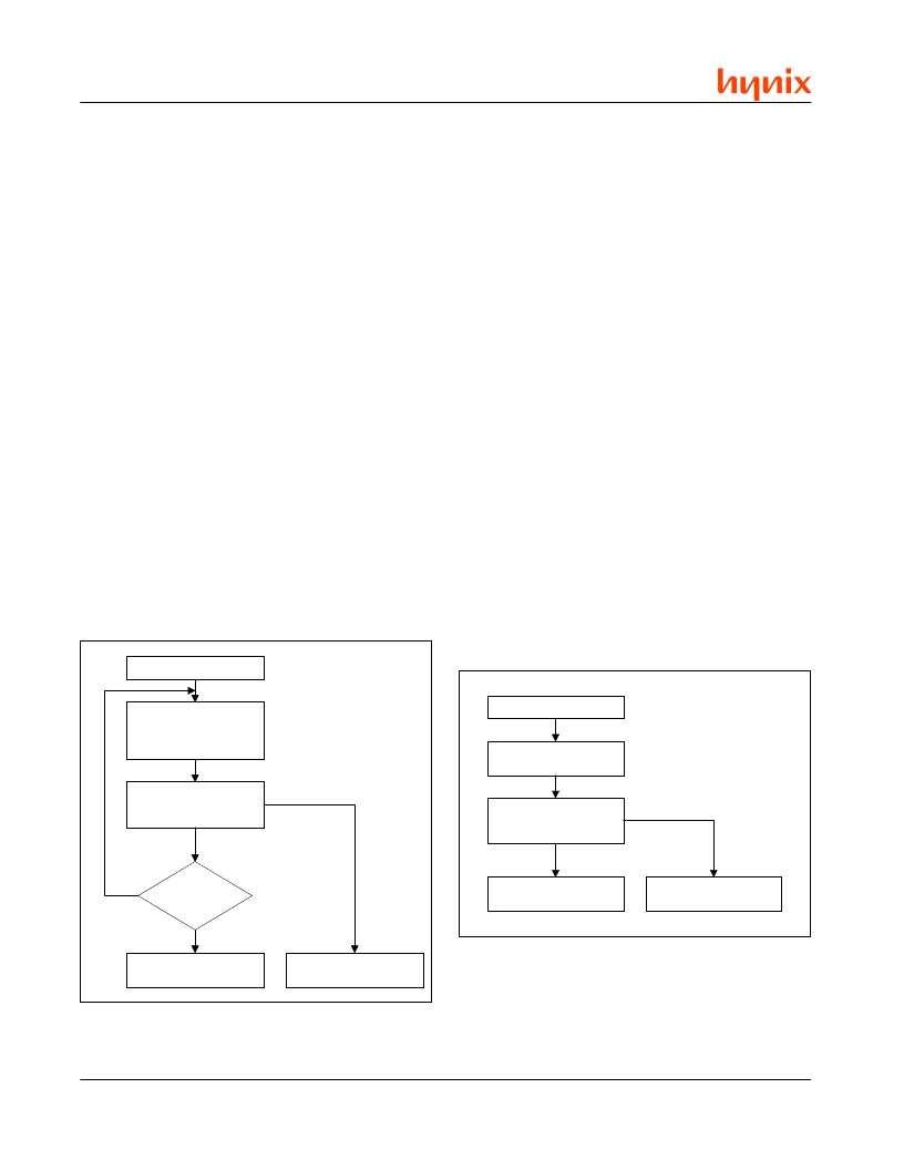
Figure 4. Programming Procedure
Figure 5. Chip Erase Procedure
Sector Erase Command
START
Issue CHIP ERASE
Command Sequence
Check Erase Status
(See Write Operation Status
Section)
CHIP ERASE COMPLETE
GO TO
ERROR RECOVERY
DQ[5] Error Exit
Normal Exit
verifies the programmed cell margin. The host is
not required to provide further controls or timings
during this operation. When the Automatic Pro-
gramming algorithm is complete, the device re-
turns to the Read mode. Several methods are
provided to allow the host to determine the status
of the programming operation, as described in the
Write Operation Status section.
Commands written to the device during execution
of the Automatic Programming algorithm are ig-
nored. Note that a hardware reset immediately
terminates the programming operation. To en-
sure data integrity, the aborted program command
sequence should be reinitiated once the reset
operation is complete.
Programming is allowed in any sequence. Only
erase operations can convert a stored
“
0
”
to a
“
1
”
.
Thus, a bit cannot be programmed from a
“
0
”
back
to a
“
1
”
. Attempting to do so will set DQ[5] to
“
1
”
,
and the Data# Polling algorithm will indicate that
the operation was not successful. A Read/Reset
command or a hardware reset is required to exit
this state, and a succeeding read will show that
the data is still
“
0
”
.
Figure 4 illustrates the procedure for the Program
operation.
Chip Erase Command
The Chip Erase command sequence consists of
two unlock cycles, followed by the erase com-
mand, two additional unlock cycles and then the
chip erase data cycle. During chip erase, all sec-
tors of the device are erased except protected
sector groups. The command sequence starts the
Automatic Erase algorithm, which preprograms
and verifies the entire memory, except for pro-
tected sector groups, for an all zero data pattern
prior to electrical erase. The device then provides
the required number of internally generated erase
pulses and verifies cell erasure within the proper
cell margins. The host system is not required to
provide any controls or timings during these op-
erations.
Commands written to the device during execution
of the Automatic Erase algorithm are ignored. Note
that a hardware reset immediately terminates the
erase operation. To ensure data integrity, the
aborted chip erase command sequence should be
reissued once the reset operation is complete.
When the Automatic Erase algorithm is finished,
the device returns to the Read mode. Several
methods are provided to allow the host to deter-
mine the status of the erase operation, as de-
scribed in the Write Operation Status section.
Figure 5 illustrates the Chip Erase procedure.
START
Issue PROGRAM
Command Sequence:
Last cycle contains
program Address/Data
Check Programming Status
(See Write Operation Status
Section)
Last Byte Done
YES
NO
PROGRAMMING
COMPLETE
GO TO
ERROR RECOVERY
DQ[5] Error Exit
Normal Exit
The Sector Erase command sequence consists
of two unlock cycles, followed by the erase com-
mand, two additional unlock cycles and then the
sector erase data cycle, which specifies which
相關(guān)PDF資料 |
PDF描述 |
|---|---|
| HY29F080T90 | 8 Megabit (1M x 8), 5 Volt-only, Flash Memory |
| HY29F080G-70 | x8 Flash EEPROM |
| HY29F080G-90 | x8 Flash EEPROM |
| HY29F080R-12 | x8 Flash EEPROM |
| HY29F080R-70 | x8 Flash EEPROM |
相關(guān)代理商/技術(shù)參數(shù) |
參數(shù)描述 |
|---|---|
| HY29F080G-12E | 制造商:未知廠家 制造商全稱:未知廠家 功能描述:x8 Flash EEPROM |
| HY29F080G-15 | 制造商:未知廠家 制造商全稱:未知廠家 功能描述:x8 Flash EEPROM |
| HY29F080G-15E | 制造商:未知廠家 制造商全稱:未知廠家 功能描述:x8 Flash EEPROM |
| HY29F080G-15I | 制造商:未知廠家 制造商全稱:未知廠家 功能描述:x8 Flash EEPROM |
| HY29F080G-55E | 制造商:未知廠家 制造商全稱:未知廠家 功能描述:x8 Flash EEPROM |
發(fā)布緊急采購,3分鐘左右您將得到回復(fù)。