- 您現在的位置:買賣IC網 > PDF目錄30730 > LC72133V (SANYO SEMICONDUCTOR CO LTD) PLL FREQUENCY SYNTHESIZER, 40 MHz, PDSO20 PDF資料下載
參數資料
| 型號: | LC72133V |
| 廠商: | SANYO SEMICONDUCTOR CO LTD |
| 元件分類: | PLL合成/DDS/VCOs |
| 英文描述: | PLL FREQUENCY SYNTHESIZER, 40 MHz, PDSO20 |
| 封裝: | SSOP-20 |
| 文件頁數: | 3/23頁 |
| 文件大小: | 147K |
| 代理商: | LC72133V |
Continued from preceding page.
No. 5427-11/23
LC72133M, 72133V
No.
Control block/data
Functions
Related data
DO pin control data
Data that determines the DO pin output
DOC0, DOC1, DOC2
The open state is selected after the power-on reset.
Note: 1. end-UC: Check for IF counter measurement completion
When end-UC is set and the IF counter is started (i.e., when CTE is changed
from zero to one), the DO pin automatically goes to the open state.
When the IF counter measurement completes, the DO pin goes low to indicate
the measurement completion state.
Depending on serial data I/O (CE: high) the DO pin goes to the open state.
2. Goes to the open state if the I/O pin is specified to be an output port.
Caution: The state of the DO pin during a data input period (an IN1 or IN2 mode period with CE
high) will be open, regardless of the state of the DO control data (DOC0 to DOC2).
Also, the DO pin during a data output period (an OUT mode period with CE high)
will output the contents of the internal DO serial data in synchronization with the
CL pin signal, regardless of the state of the DO control data (DOC0 to DOC2).
Unlock detection data
Selects the phase error (E) detection width for checking PLL lock.
UL0, UL1
A phase error in excess of the specified detection width is seen as an unlocked state.
Note: In the unlocked state the DO pin goes low and the UL bit in the serial data
becomes zero.
Phase comparator
Controls the phase comparator dead zone.
control data
DZ0, DZ1
Dead zone widths: DZA < DZB < DZC < DZD
Clock time base
Setting TBC to one causes an 8 Hz, 40% duty clock time base signal to be output
TBC
from the BO1 pin. (BO1 data is invalid in this mode.)
Charge pump control data
Forcibly controls the charge pump output.
DLC
Note: If deadlock occurs due to the VCO control voltage (Vtune) going to zero and the VCO
oscillator stopping, deadlock can be cleared by forcing the charge pump output to
low and setting Vtune to VCC. (This is the deadlock clearing circuit.)
(6)
(7)
(8)
(9)
(10)
UL0, UL1,
CTE,
IOC1, IOC2
DOC0,
DOC1,
DOC2
BO1
DOC2
DOC1
DOC0
DO pin state
0
Open
0
1
Low when the unlock state is detected
0
1
0
end-UC*1
0
1
Open
1
0
Open
1
0
1
The IO1 pin state*2
1
0
The IO2 pin state*2
1
Open
UL1
UL0
E detection width
Detector output
0
Stopped
Open
0
1
0
E is output directly
1
0
±0.55 s
E is extended by 1 to 2 ms
1
±1.11
E is extended by 1 to 2 ms
DZ1
DZ0
Dead zone mode
0
DZA
0
1
DZB
1
0
DZC
1
DZD
DLC
Charge pump output
0
Normal operation
1
Forced low
Continued on next page.
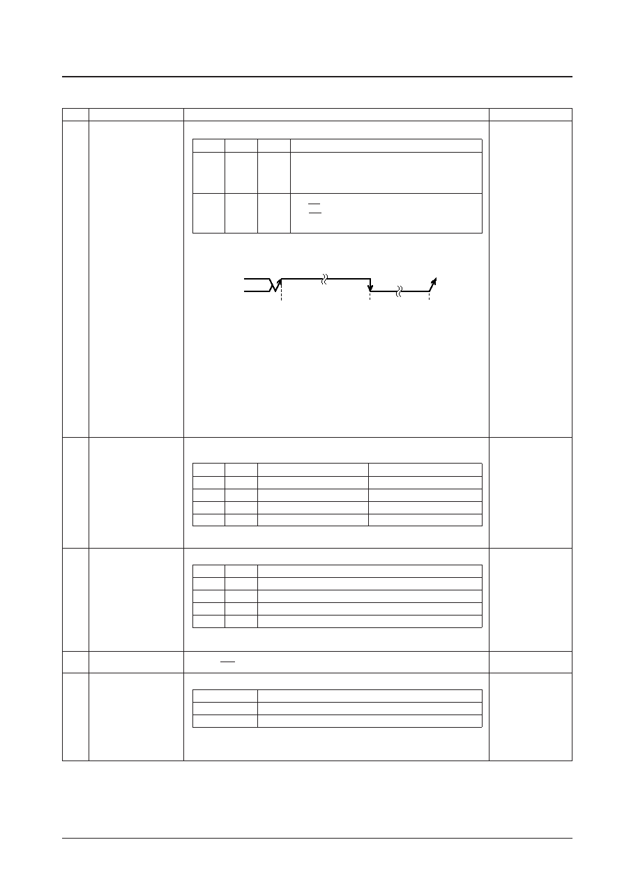
DO pin
Counter start
Counter
complete
CE: high
A11920
相關PDF資料 |
PDF描述 |
|---|---|
| LC72133M | PLL FREQUENCY SYNTHESIZER, 40 MHz, PDSO20 |
| LC7219M | PLL FREQUENCY SYNTHESIZER, 160 MHz, PDSO24 |
| LC7230-8221 | SPECIALTY CONSUMER CIRCUIT, PQFP80 |
| LC7230-8272 | SPECIALTY CONSUMER CIRCUIT, PQFP80 |
| LC72323-XXXX | SPECIALTY CONSUMER CIRCUIT, PQFP80 |
相關代理商/技術參數 |
參數描述 |
|---|---|
| LC72133V-TLM-E | 制造商:ON Semiconductor 功能描述:PLL FREQUENCY SYNTHESIZER - Tape and Reel |
| LC72134M | 制造商:SANYO 制造商全稱:Sanyo Semicon Device 功能描述:Dual PLL Frequency Synthesizer for FM Tuner Systems |
| LC72135M | 制造商:SANYO 制造商全稱:Sanyo Semicon Device 功能描述:PLL Frequency Synthesizer for Electronic Tuning |
| LC72135MA-AE | 功能描述:時鐘合成器/抖動清除器 RoHS:否 制造商:Skyworks Solutions, Inc. 輸出端數量: 輸出電平: 最大輸出頻率: 輸入電平: 最大輸入頻率:6.1 GHz 電源電壓-最大:3.3 V 電源電壓-最小:2.7 V 封裝 / 箱體:TSSOP-28 封裝:Reel |
| LC72135MA-Q-AE | 制造商:ON Semiconductor 功能描述:PLL FREQUENCY SYNTHESIZER - Tape and Reel 制造商:ON Semiconductor 功能描述:REEL / PLL FREQUENCY SYNTHESIZER |
發布緊急采購,3分鐘左右您將得到回復。