- 您現在的位置:買賣IC網 > PDF目錄21974 > LFX125EB-03F256C (Lattice Semiconductor Corporation)IC FPGA 139K GATES 256-BGA PDF資料下載
參數資料
| 型號: | LFX125EB-03F256C |
| 廠商: | Lattice Semiconductor Corporation |
| 文件頁數: | 26/119頁 |
| 文件大小: | 0K |
| 描述: | IC FPGA 139K GATES 256-BGA |
| 標準包裝: | 90 |
| 系列: | ispXPGA® |
| 邏輯元件/單元數: | 1936 |
| RAM 位總計: | 94208 |
| 輸入/輸出數: | 160 |
| 門數: | 139000 |
| 電源電壓: | 2.3 V ~ 3.6 V |
| 安裝類型: | 表面貼裝 |
| 工作溫度: | 0°C ~ 85°C |
| 封裝/外殼: | 256-BGA |
| 供應商設備封裝: | 256-FPBGA(17x17) |
| 其它名稱: | 220-1237 |
第1頁第2頁第3頁第4頁第5頁第6頁第7頁第8頁第9頁第10頁第11頁第12頁第13頁第14頁第15頁第16頁第17頁第18頁第19頁第20頁第21頁第22頁第23頁第24頁第25頁當前第26頁第27頁第28頁第29頁第30頁第31頁第32頁第33頁第34頁第35頁第36頁第37頁第38頁第39頁第40頁第41頁第42頁第43頁第44頁第45頁第46頁第47頁第48頁第49頁第50頁第51頁第52頁第53頁第54頁第55頁第56頁第57頁第58頁第59頁第60頁第61頁第62頁第63頁第64頁第65頁第66頁第67頁第68頁第69頁第70頁第71頁第72頁第73頁第74頁第75頁第76頁第77頁第78頁第79頁第80頁第81頁第82頁第83頁第84頁第85頁第86頁第87頁第88頁第89頁第90頁第91頁第92頁第93頁第94頁第95頁第96頁第97頁第98頁第99頁第100頁第101頁第102頁第103頁第104頁第105頁第106頁第107頁第108頁第109頁第110頁第111頁第112頁第113頁第114頁第115頁第116頁第117頁第118頁第119頁
Lattice Semiconductor
ispXPGA Family Data Sheet
10
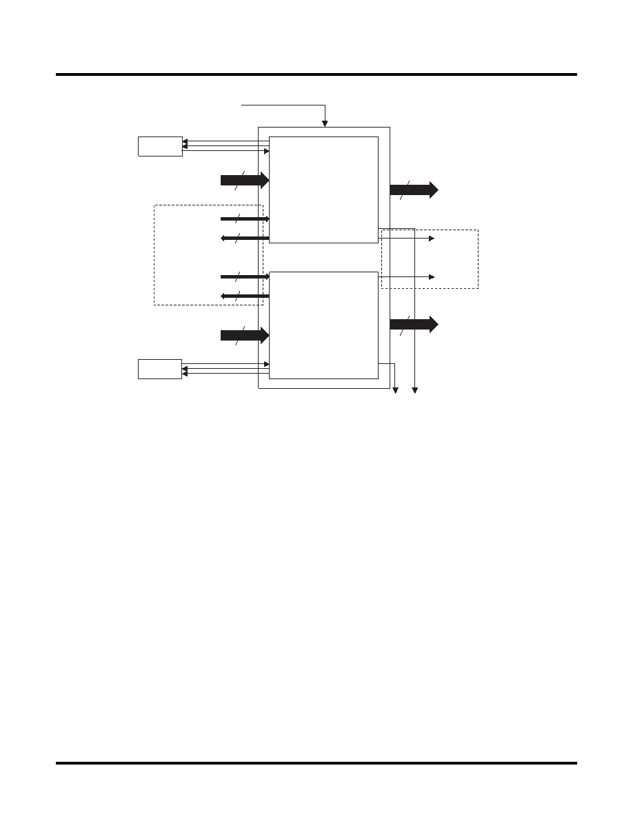
Figure 10. ispXPGA PIC
Programmable Input/Output
The PIO is the building block of a PIC. The PIO has a total of 11 inputs and five outputs. Nine of the 11 inputs are
generated from routing. The inputs from routing are the PIO Input (IN), Feed-Thru (FT), Clock (CLK), Input Clock
Enable (ICE), Input Set/Reset (ISR), Output Clock Enable (OCEN), Output Set/Reset (OSR), PIO Output Enable
(OEN), and PIO Input Enable (IEN). The remaining inputs are the sysIO input buffer signal and the Global Set/
Reset signal. Three of the five outputs (OUT0, OUT1, and OE) feed routing. The last two outputs feed the sysIO
buffer directly as the output and output enable of the sysIO output buffer.
PIOs associated with sysHSI blocks contain two additional inputs and outputs to support the sysHSI block. The two
inputs come from the sysHSI block associated with the PIO, and the two outputs feed the sysHSI block. One of the
inputs routes directly through the PIO to routing, while the other is multiplexed with the Feed-Thru, register bypass,
and Q output of the register to form the OUT1 output of the PIO. The outputs to the sysHSI block are the same sig-
nals as the outputs which feed the sysIO buffers (sysIO Output and sysIO Output Enable).
Each PIO has an input register, an output register, and an output enable register as shown in Figure 11. The input
register path of the PIO has a ‘delay’ option, which slows the data-flow. A two-input OR function of the Global Set/
Reset (GSR) and Set/Reset (ISR or OSR) signals creates the set/reset term for the respective registers. Each PIO
has two pairs of set/reset and clock enable signals. One is exclusive to the input register, whereas the other is com-
mon for both the output and output enable registers. The clock (CLK) is common to all registers in a PIO, and the
polarity of the clock is controllable. The input, output, and the output enable registers can be configured as a latch
or D-type flip-flop. Each PIO is capable of generating an output enable signal, which in turn becomes a PIC output.
PIC
PIO0
PIO1
OE1 OE0
sysIO
9
2
To routing
Only for PICs
associated with
sysHSI blocks
Only for PICs
associated with
sysHSI blocks
To routing
From routing
GSR
sysIO
From sysHSI block
To sysHSI block
2
9
From sysHSI block
To sysHSI block
2
SELECT
DEVICES
DISCONTINUED
相關PDF資料 |
PDF描述 |
|---|---|
| UBA2015AT/1,118 | IC LAMP DVR FLUORES 600V 20-SOIC |
| LFEC15E-3FN484C | IC FPGA 10.2KLUTS 288I/O 484-BGA |
| REC3-1215DRW/H2/A | CONV DC/DC 3W 9-18VIN +/-15VOUT |
| DAPV15P565GTXLF | CONN DSUB PLUG 15POS R/A PCB |
| AIML-0603-100K-T | INDUCTOR MULTILAYER 10000NH 0603 |
相關代理商/技術參數 |
參數描述 |
|---|---|
| LFX125EB-03F256I | 功能描述:FPGA - 現場可編程門陣列 139K Gates, 160 I/O 2.5/3.3V, -3 speed RoHS:否 制造商:Altera Corporation 系列:Cyclone V E 柵極數量: 邏輯塊數量:943 內嵌式塊RAM - EBR:1956 kbit 輸入/輸出端數量:128 最大工作頻率:800 MHz 工作電源電壓:1.1 V 最大工作溫度:+ 70 C 安裝風格:SMD/SMT 封裝 / 箱體:FBGA-256 |
| LFX125EB-03F516C | 功能描述:FPGA - 現場可編程門陣列 139K 176 I/O ispJTAG RoHS:否 制造商:Altera Corporation 系列:Cyclone V E 柵極數量: 邏輯塊數量:943 內嵌式塊RAM - EBR:1956 kbit 輸入/輸出端數量:128 最大工作頻率:800 MHz 工作電源電壓:1.1 V 最大工作溫度:+ 70 C 安裝風格:SMD/SMT 封裝 / 箱體:FBGA-256 |
| LFX125EB-03F516I | 功能描述:FPGA - 現場可編程門陣列 139K 176 I/O ispJTAG RoHS:否 制造商:Altera Corporation 系列:Cyclone V E 柵極數量: 邏輯塊數量:943 內嵌式塊RAM - EBR:1956 kbit 輸入/輸出端數量:128 最大工作頻率:800 MHz 工作電源電壓:1.1 V 最大工作溫度:+ 70 C 安裝風格:SMD/SMT 封裝 / 箱體:FBGA-256 |
| LFX125EB-03FH516C | 功能描述:FPGA - 現場可編程門陣列 Use LFX125EB-03F516C RoHS:否 制造商:Altera Corporation 系列:Cyclone V E 柵極數量: 邏輯塊數量:943 內嵌式塊RAM - EBR:1956 kbit 輸入/輸出端數量:128 最大工作頻率:800 MHz 工作電源電壓:1.1 V 最大工作溫度:+ 70 C 安裝風格:SMD/SMT 封裝 / 箱體:FBGA-256 |
| LFX125EB-03FH516I | 功能描述:FPGA - 現場可編程門陣列 Use LFX125EB-03F516I RoHS:否 制造商:Altera Corporation 系列:Cyclone V E 柵極數量: 邏輯塊數量:943 內嵌式塊RAM - EBR:1956 kbit 輸入/輸出端數量:128 最大工作頻率:800 MHz 工作電源電壓:1.1 V 最大工作溫度:+ 70 C 安裝風格:SMD/SMT 封裝 / 箱體:FBGA-256 |
發布緊急采購,3分鐘左右您將得到回復。