- 您現在的位置:買賣IC網 > PDF目錄21974 > LFX125EB-03F256C (Lattice Semiconductor Corporation)IC FPGA 139K GATES 256-BGA PDF資料下載
參數資料
| 型號: | LFX125EB-03F256C |
| 廠商: | Lattice Semiconductor Corporation |
| 文件頁數: | 30/119頁 |
| 文件大小: | 0K |
| 描述: | IC FPGA 139K GATES 256-BGA |
| 標準包裝: | 90 |
| 系列: | ispXPGA® |
| 邏輯元件/單元數: | 1936 |
| RAM 位總計: | 94208 |
| 輸入/輸出數: | 160 |
| 門數: | 139000 |
| 電源電壓: | 2.3 V ~ 3.6 V |
| 安裝類型: | 表面貼裝 |
| 工作溫度: | 0°C ~ 85°C |
| 封裝/外殼: | 256-BGA |
| 供應商設備封裝: | 256-FPBGA(17x17) |
| 其它名稱: | 220-1237 |
第1頁第2頁第3頁第4頁第5頁第6頁第7頁第8頁第9頁第10頁第11頁第12頁第13頁第14頁第15頁第16頁第17頁第18頁第19頁第20頁第21頁第22頁第23頁第24頁第25頁第26頁第27頁第28頁第29頁當前第30頁第31頁第32頁第33頁第34頁第35頁第36頁第37頁第38頁第39頁第40頁第41頁第42頁第43頁第44頁第45頁第46頁第47頁第48頁第49頁第50頁第51頁第52頁第53頁第54頁第55頁第56頁第57頁第58頁第59頁第60頁第61頁第62頁第63頁第64頁第65頁第66頁第67頁第68頁第69頁第70頁第71頁第72頁第73頁第74頁第75頁第76頁第77頁第78頁第79頁第80頁第81頁第82頁第83頁第84頁第85頁第86頁第87頁第88頁第89頁第90頁第91頁第92頁第93頁第94頁第95頁第96頁第97頁第98頁第99頁第100頁第101頁第102頁第103頁第104頁第105頁第106頁第107頁第108頁第109頁第110頁第111頁第112頁第113頁第114頁第115頁第116頁第117頁第118頁第119頁
Lattice Semiconductor
ispXPGA Family Data Sheet
14
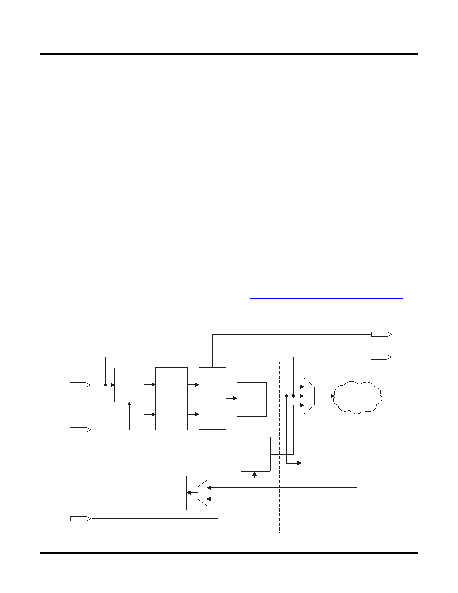
sysCLOCK PLL Description
The sysCLOCK PLL circuitry consists of Phase-Lock Loops (PLLs) and the various dividers, reset, and feedback
signals associated with the PLLs. This feature gives the user the ability to synthesize clock frequencies and gener-
ate multiple clock signals for routing within the device. Furthermore, it can generate clock signals that are aligned
either at the board level or the device level.
The ispXPGA devices provide up to eight PLLs. Each PLL receives its input clock from its associated global clock
pin, and its output is routed to the associated global clock net. For example, PLL0 receives its clock input from the
GCLK0 global clock pin and provides output to the CLK0 global clock net. The PLL also has the ability to output a
secondary clock that is a division of the primary clock output. When using the secondary clock, the secondary
clock will be routed to the neighboring global clock net. For example, PLL0 will drive its primary clock output on the
CLK0 global clock net and its secondary clock output will drive the CLK1 global clock net. Additionally, each PLL
has a set of PLL_RST, PLL_FBK, and PLL_LOCK signals. The PLL_RST signal can be generated through routing
or a dedicated dual-function I/O pin. The PLL_FBK signal can be generated through a dedicated dual-function I/O
pin or internally from the Global Clock net associated with the PLL. The PLL_LOCK signal feeds routing directly
from the sysCLOCK PLL circuit. Figure 17 illustrates how the PLL_RST and PLL_FBK signals are generated.
Each PLL has four dividers associated with it, M, N, V, and K. The M divider is used to divide the clock signal,
while the N divider is used to multiply the clock signal. The V divider allows the VCO frequency to operate at
higher frequencies than the clock output, thereby increasing the frequency range. The K divider is only used when
a secondary clock output is needed. This divider divides the primary clock output and feeds to the adjacent global
clock net. Different combinations of these dividers allow the user to synthesize clock frequencies. Figure 16 shows
the ispXPGA PLL block diagram.
The PLL also has a delay feature that allows the output clock to be advanced or delayed to improve set-up and
clock-to-out times for better performance. This operates by inserting delay on the input or feedback lines of the
PLL. For more information on the PLL, please refer to TN1003, sysCLOCK PLL Usage and Design Guidelines.
Figure 16. ispXPGA PLL Block Diagram
GCLK_IN
PLL_RST
PLL_FBK
PLL_LOCK
CLK_OUT
Clock Net
Input Clock
(M) Divider
÷ 1 to 32
PLL (n)
Programmable
+Delay
--------------------
Programmable
-Delay
To Adjacent_PLL
Feedback
Divider (N)
X 1 to 32
Post-scalar
(V) Divider
÷
1, 2, 4, 8,
16, 32
Clock (K)
Divider
÷
2, 4, 8,
16, 32
From
Adjacent_PLL
SELECT
DEVICES
DISCONTINUED
相關PDF資料 |
PDF描述 |
|---|---|
| UBA2015AT/1,118 | IC LAMP DVR FLUORES 600V 20-SOIC |
| LFEC15E-3FN484C | IC FPGA 10.2KLUTS 288I/O 484-BGA |
| REC3-1215DRW/H2/A | CONV DC/DC 3W 9-18VIN +/-15VOUT |
| DAPV15P565GTXLF | CONN DSUB PLUG 15POS R/A PCB |
| AIML-0603-100K-T | INDUCTOR MULTILAYER 10000NH 0603 |
相關代理商/技術參數 |
參數描述 |
|---|---|
| LFX125EB-03F256I | 功能描述:FPGA - 現場可編程門陣列 139K Gates, 160 I/O 2.5/3.3V, -3 speed RoHS:否 制造商:Altera Corporation 系列:Cyclone V E 柵極數量: 邏輯塊數量:943 內嵌式塊RAM - EBR:1956 kbit 輸入/輸出端數量:128 最大工作頻率:800 MHz 工作電源電壓:1.1 V 最大工作溫度:+ 70 C 安裝風格:SMD/SMT 封裝 / 箱體:FBGA-256 |
| LFX125EB-03F516C | 功能描述:FPGA - 現場可編程門陣列 139K 176 I/O ispJTAG RoHS:否 制造商:Altera Corporation 系列:Cyclone V E 柵極數量: 邏輯塊數量:943 內嵌式塊RAM - EBR:1956 kbit 輸入/輸出端數量:128 最大工作頻率:800 MHz 工作電源電壓:1.1 V 最大工作溫度:+ 70 C 安裝風格:SMD/SMT 封裝 / 箱體:FBGA-256 |
| LFX125EB-03F516I | 功能描述:FPGA - 現場可編程門陣列 139K 176 I/O ispJTAG RoHS:否 制造商:Altera Corporation 系列:Cyclone V E 柵極數量: 邏輯塊數量:943 內嵌式塊RAM - EBR:1956 kbit 輸入/輸出端數量:128 最大工作頻率:800 MHz 工作電源電壓:1.1 V 最大工作溫度:+ 70 C 安裝風格:SMD/SMT 封裝 / 箱體:FBGA-256 |
| LFX125EB-03FH516C | 功能描述:FPGA - 現場可編程門陣列 Use LFX125EB-03F516C RoHS:否 制造商:Altera Corporation 系列:Cyclone V E 柵極數量: 邏輯塊數量:943 內嵌式塊RAM - EBR:1956 kbit 輸入/輸出端數量:128 最大工作頻率:800 MHz 工作電源電壓:1.1 V 最大工作溫度:+ 70 C 安裝風格:SMD/SMT 封裝 / 箱體:FBGA-256 |
| LFX125EB-03FH516I | 功能描述:FPGA - 現場可編程門陣列 Use LFX125EB-03F516I RoHS:否 制造商:Altera Corporation 系列:Cyclone V E 柵極數量: 邏輯塊數量:943 內嵌式塊RAM - EBR:1956 kbit 輸入/輸出端數量:128 最大工作頻率:800 MHz 工作電源電壓:1.1 V 最大工作溫度:+ 70 C 安裝風格:SMD/SMT 封裝 / 箱體:FBGA-256 |
發布緊急采購,3分鐘左右您將得到回復。