- 您現在的位置:買賣IC網 > PDF目錄21974 > LFX125EB-03F256C (Lattice Semiconductor Corporation)IC FPGA 139K GATES 256-BGA PDF資料下載
參數資料
| 型號: | LFX125EB-03F256C |
| 廠商: | Lattice Semiconductor Corporation |
| 文件頁數: | 71/119頁 |
| 文件大小: | 0K |
| 描述: | IC FPGA 139K GATES 256-BGA |
| 標準包裝: | 90 |
| 系列: | ispXPGA® |
| 邏輯元件/單元數: | 1936 |
| RAM 位總計: | 94208 |
| 輸入/輸出數: | 160 |
| 門數: | 139000 |
| 電源電壓: | 2.3 V ~ 3.6 V |
| 安裝類型: | 表面貼裝 |
| 工作溫度: | 0°C ~ 85°C |
| 封裝/外殼: | 256-BGA |
| 供應商設備封裝: | 256-FPBGA(17x17) |
| 其它名稱: | 220-1237 |
第1頁第2頁第3頁第4頁第5頁第6頁第7頁第8頁第9頁第10頁第11頁第12頁第13頁第14頁第15頁第16頁第17頁第18頁第19頁第20頁第21頁第22頁第23頁第24頁第25頁第26頁第27頁第28頁第29頁第30頁第31頁第32頁第33頁第34頁第35頁第36頁第37頁第38頁第39頁第40頁第41頁第42頁第43頁第44頁第45頁第46頁第47頁第48頁第49頁第50頁第51頁第52頁第53頁第54頁第55頁第56頁第57頁第58頁第59頁第60頁第61頁第62頁第63頁第64頁第65頁第66頁第67頁第68頁第69頁第70頁當前第71頁第72頁第73頁第74頁第75頁第76頁第77頁第78頁第79頁第80頁第81頁第82頁第83頁第84頁第85頁第86頁第87頁第88頁第89頁第90頁第91頁第92頁第93頁第94頁第95頁第96頁第97頁第98頁第99頁第100頁第101頁第102頁第103頁第104頁第105頁第106頁第107頁第108頁第109頁第110頁第111頁第112頁第113頁第114頁第115頁第116頁第117頁第118頁第119頁
Lattice Semiconductor
ispXPGA Family Data Sheet
51
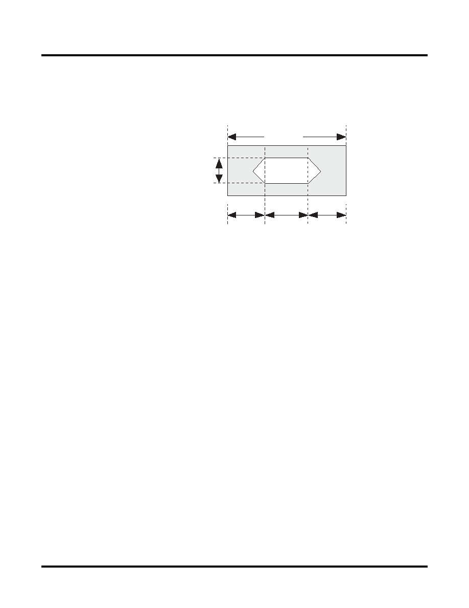
sysHSI Block Timing
Figure 24 provides a graphical representation of the SERDES receiver input requirements. It provides guidance on
a number of input parameters, including signal amplitude and rise time limits, noise and jitter limits, and P and N
input skew tolerance.
Figure 24. Receive Data Eye Diagram Template (Differential)
The data pattern eye opening at the receive end of a link is considered the ultimate measure of received signal
quality. Almost all detrimental characteristics of a transmit signal and the interconnection link design result in eye
closure. This combined with the eye-opening limitations of the line receiver can provide a good indication of a link’s
ability to transfer error-free data.
Signal jitter is of special interest to system designers. It is often the primary limiting characteristic of long digital
links and of systems with high noise level environments. An interesting characteristic of the clock and data recovery
(CDR) portion of the ispXPGA SERDES receiver is its ability to filter incoming signal jitter that is below the clock
recovery PLL bandwidth. For signals with high levels of low frequency jitter, the receiver can detect incoming data
error free, with eye openings significantly less than that shown in Figure 24.
eo
SIN
V
THD
200 mV Differential
+/- 100 mV Single Ended
jt
TH
Bit Time
jt
TH : Optimum Threshold Crossing Jitter
jt
TH
SELECT
DEVICES
DISCONTINUED
相關PDF資料 |
PDF描述 |
|---|---|
| UBA2015AT/1,118 | IC LAMP DVR FLUORES 600V 20-SOIC |
| LFEC15E-3FN484C | IC FPGA 10.2KLUTS 288I/O 484-BGA |
| REC3-1215DRW/H2/A | CONV DC/DC 3W 9-18VIN +/-15VOUT |
| DAPV15P565GTXLF | CONN DSUB PLUG 15POS R/A PCB |
| AIML-0603-100K-T | INDUCTOR MULTILAYER 10000NH 0603 |
相關代理商/技術參數 |
參數描述 |
|---|---|
| LFX125EB-03F256I | 功能描述:FPGA - 現場可編程門陣列 139K Gates, 160 I/O 2.5/3.3V, -3 speed RoHS:否 制造商:Altera Corporation 系列:Cyclone V E 柵極數量: 邏輯塊數量:943 內嵌式塊RAM - EBR:1956 kbit 輸入/輸出端數量:128 最大工作頻率:800 MHz 工作電源電壓:1.1 V 最大工作溫度:+ 70 C 安裝風格:SMD/SMT 封裝 / 箱體:FBGA-256 |
| LFX125EB-03F516C | 功能描述:FPGA - 現場可編程門陣列 139K 176 I/O ispJTAG RoHS:否 制造商:Altera Corporation 系列:Cyclone V E 柵極數量: 邏輯塊數量:943 內嵌式塊RAM - EBR:1956 kbit 輸入/輸出端數量:128 最大工作頻率:800 MHz 工作電源電壓:1.1 V 最大工作溫度:+ 70 C 安裝風格:SMD/SMT 封裝 / 箱體:FBGA-256 |
| LFX125EB-03F516I | 功能描述:FPGA - 現場可編程門陣列 139K 176 I/O ispJTAG RoHS:否 制造商:Altera Corporation 系列:Cyclone V E 柵極數量: 邏輯塊數量:943 內嵌式塊RAM - EBR:1956 kbit 輸入/輸出端數量:128 最大工作頻率:800 MHz 工作電源電壓:1.1 V 最大工作溫度:+ 70 C 安裝風格:SMD/SMT 封裝 / 箱體:FBGA-256 |
| LFX125EB-03FH516C | 功能描述:FPGA - 現場可編程門陣列 Use LFX125EB-03F516C RoHS:否 制造商:Altera Corporation 系列:Cyclone V E 柵極數量: 邏輯塊數量:943 內嵌式塊RAM - EBR:1956 kbit 輸入/輸出端數量:128 最大工作頻率:800 MHz 工作電源電壓:1.1 V 最大工作溫度:+ 70 C 安裝風格:SMD/SMT 封裝 / 箱體:FBGA-256 |
| LFX125EB-03FH516I | 功能描述:FPGA - 現場可編程門陣列 Use LFX125EB-03F516I RoHS:否 制造商:Altera Corporation 系列:Cyclone V E 柵極數量: 邏輯塊數量:943 內嵌式塊RAM - EBR:1956 kbit 輸入/輸出端數量:128 最大工作頻率:800 MHz 工作電源電壓:1.1 V 最大工作溫度:+ 70 C 安裝風格:SMD/SMT 封裝 / 箱體:FBGA-256 |
發布緊急采購,3分鐘左右您將得到回復。