- 您現在的位置:買賣IC網 > PDF目錄382345 > MPC603E7TEC (Motorola, Inc.) PowerPC 603e RISC Microprocessor PDF資料下載
參數資料
| 型號: | MPC603E7TEC |
| 廠商: | Motorola, Inc. |
| 英文描述: | PowerPC 603e RISC Microprocessor |
| 中文描述: | RISC微處理器的PowerPC 603e |
| 文件頁數: | 9/36頁 |
| 文件大?。?/td> | 551K |
| 代理商: | MPC603E7TEC |
第1頁第2頁第3頁第4頁第5頁第6頁第7頁第8頁當前第9頁第10頁第11頁第12頁第13頁第14頁第15頁第16頁第17頁第18頁第19頁第20頁第21頁第22頁第23頁第24頁第25頁第26頁第27頁第28頁第29頁第30頁第31頁第32頁第33頁第34頁第35頁第36頁
PID7t-603e Hardware Specifications
For More Information On This Product,
Go to: www.freescale.com
9
Electrical and Thermal Characteristics
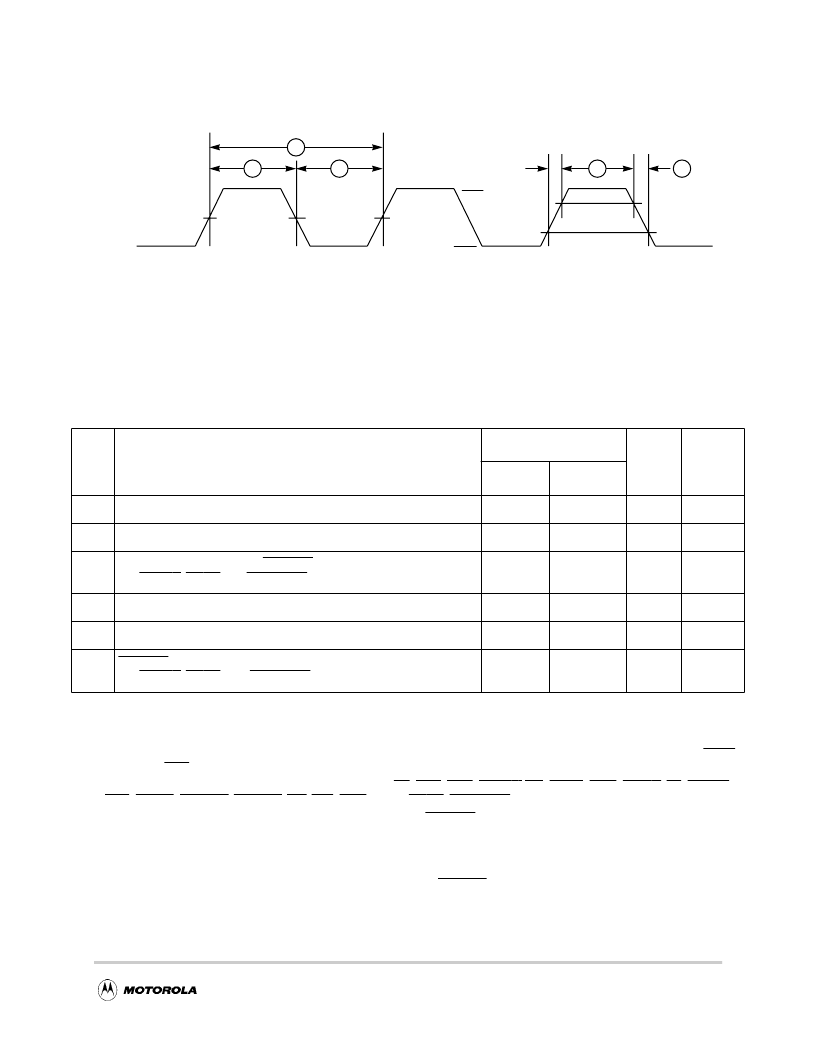
Figure 1 provides the SYSCLK input timing diagram.
Figure 1. SYSCLK Input Timing Diagram
1.4.2.2 Input AC SpeciTcations
Table 8 provides the input AC timing speciTcations for the PID7t-603e as deTned in Figure 2 and Figure 3.
Table 8. Input AC Timing Specifications
1
Vdd = AVdd = 2.5 ± 5% V dc, OVdd = 3.3 ± 5% V dc, GND = 0 V dc
,
0
£
Tj
£
105° C
Num
Characteristic
200, 266, 300 MHz
Unit
Notes
Min
Max
10a
Address/data/transfer attribute inputs valid to SYSCLK (input setup)
2.5
—
ns
2
10b
All other inputs valid to SYSCLK (input setup)
3.5
—
ns
3
10c
Mode select inputs valid to HRESET (input setup)
(for DRTRY, QACK and TLBISYNC)
8
—
t
sysclk
4, 5, 6, 7
11a
SYSCLK to address/data/transfer attribute inputs invalid (input hold)
1.0
—
ns
2
11b
SYSCLK to all other inputs invalid (input hold)
1.0
—
ns
3
11c
HRESET to mode select inputs invalid (input hold)
(for DRTRY, QACK, and TLBISYNC)
0
—
ns
4, 6, 7
Note
1. Input specifications are measured from the TTL level (0.8 or 2.0 V) of the signal in question to the 1.4 V of the rising edge
of the input SYSCLK. Input and output timings are measured at the pin.
2. Address/data/transfer attribute input signals are composed of the following—A[0–31], AP[0–3], TT[0–4], TC[0–1], TBST,
TSIZ[0–2], GBL, DH[0–31], DL[0–31], DP[0–7].
3. All other input signals are composed of the following—TS, ABB, DBB, ARTRY, BG, AACK, DBG, DBWO, TA, DRTRY,
TEA, DBDIS, HRESET, SRESET, INT, SMI, MCP, TBEN, QACK, TLBISYNC.
4. The setup and hold time is with respect to the rising edge of HRESET (see Figure 3).
5. t
sysclk
is the period of the external clock (SYSCLK) in nanoseconds (ns). The numbers given in the table must be
multiplied by the period of SYSCLK to compute the actual time duration (in nanoseconds) of the parameter in question.
6. These values are guaranteed by design, and are not tested.
7. This specification is for configuration mode only. Also note that HRESET must be held asserted for a minimum of 255
bus clocks after the PLL-relock time during the power-on reset sequence.
s:
VM
CVil
CVih
SYSCLK
2
3
4
VM = Midpoint Voltage (1.4 V)
4
1
VM
VM
F
Freescale Semiconductor, Inc.
n
.
相關PDF資料 |
PDF描述 |
|---|---|
| MPC603E7TED | PowerPC 603e RISC Microprocessor |
| MPC750 | Hall Effect Switch IC; Package/Case:3-SOT-23; Supply Voltage Max:24V; Current Rating:4mA; Leaded Process Compatible:Yes; Operate Point Max:90G; Operate Point Min:-90G; Operational Type:Latch; Peak Reflow Compatible (260 C):Yes RoHS Compliant: Yes |
| MPC823 | Communication Processor Module |
| MPC823UM_REV1_16-CPM7 | 10 AMP SUBMINIATURE POWER RELAY |
| MPC9109 | LOW VOLTAGE 1:18 CLOCK DISTRIBUTION CHIP |
相關代理商/技術參數 |
參數描述 |
|---|---|
| MPC603E7TED | 制造商:MOTOROLA 制造商全稱:Motorola, Inc 功能描述:PowerPC 603e RISC Microprocessor |
| mpc603efe100ln | 制造商: 功能描述: 制造商:undefined 功能描述: |
| MPC603EFE100TN | 制造商:未知廠家 制造商全稱:未知廠家 功能描述:PowerPC 603e RISC Microprocessor Family: PID6-603e (Stretch) Part Number Specifications |
| MPC603EFE133LN | 制造商:Motorola Inc 功能描述: |
| MPC603EFE133TN | 制造商:未知廠家 制造商全稱:未知廠家 功能描述:PowerPC 603e RISC Microprocessor Family: PID6-603e (Stretch) Part Number Specifications |
發布緊急采購,3分鐘左右您將得到回復。