- 您現在的位置:買賣IC網 > PDF目錄382345 > MPC9448 (Motorola, Inc.) 3.3V/2.5V LVCMOS 1:12 Clock Fanout Buffer PDF資料下載
參數資料
| 型號: | MPC9448 |
| 廠商: | Motorola, Inc. |
| 英文描述: | 3.3V/2.5V LVCMOS 1:12 Clock Fanout Buffer |
| 中文描述: | 3.3V/2.5V的LVCMOS 1:12時鐘扇出緩沖器 |
| 文件頁數: | 5/12頁 |
| 文件大小: | 263K |
| 代理商: | MPC9448 |
MPC9448
TIMING SOLUTIONS
5
MOTOROLA
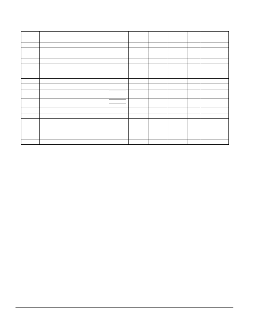
Table 8. AC CHARACTERISTICS
(V
CC
= 2.5V
±
5%, T
A
= --40
°
C to +85
°
C)
a
Symbol
Characteristics
f
ref
Input Frequency
f
MAX
Maximum Output Frequency
V
PP
Peak-to-peak input voltage
V
CMRb
Common Mode Range
t
P, REF
Reference Input Pulse Width
t
r
, t
f
CCLK Input Rise/Fall Time
t
PLH/HL
t
PLH/HL
t
PLZ, HZ
Output Disable Time
t
PZL, LZ
Output Enable Time
t
S
Setup time
Min
0
0
400
1.2
1.4
Typ
Max
350
350
1000
V
CC
-0.8
Unit
MHz
MHz
mV
V
ns
ns
ns
ns
ns
ns
ns
ns
ns
ns
ps
ns
ps
ps
Condition
PCLK
PCLK
LVPECL
LVPECL
1.0
c
4.2
4.4
11
11
0.8 to 2.0V
Propagation delay
PCLK to any Q
CCLK to any Q
1.5
1.7
CCLK to CLK_STOP
PCLK to CLK_STOP
CCLK to CLK_STOP
PCLK to CLK_STOP
0.0
0.0
1.0
1.5
t
H
Hold time
t
sk(O)
t
sk(PP)
t
SK(p)
Output-to-output Skew
Device-to-device Skew
Output pulse skew
d
150
2.7
200
300
PCLK or CCLK to any Q
Using CCLK
Using PCLK
DC
Q
Output Duty Cycle
f
Q
< 350 MHz and using CCLK
f
Q
<200 MHz and using PCLK
45
45
0.1
50
50
55
55
1.0
%
%
ns
DC
REF
= 50%
t
r
, t
f
Output Rise/Fall Time
0.6 to 1.8V
a. AC characteristics apply for parallel output termination of 50
to V
TT
.
b. V
CMR
(AC) is the crosspoint of the differential input signal. Normal AC operation is obtained when the crosspoint is within the V
CMR
range
and the input swing lies within the V
PP
(AC) specification. Violation of V
CMR
or V
PP
impacts t
PLH/HL
and t
SK(PP)
.
c. Violation of the 1.0 ns maximum input rise and fall time limit will affect the device propagation delay, device-to-device skew, reference input
pulse width, output duty cycle and maximum frequency specifications.
d. Output pulse skew is the absolute difference of the propagation delay times: | t
pLH
- t
pHL
|.
F
Freescale Semiconductor, Inc.
For More Information On This Product,
Go to: www.freescale.com
n
.
相關PDF資料 |
PDF描述 |
|---|---|
| MPC9448D | 3.3V/2.5V LVCMOS 1:12 Clock Fanout Buffer |
| MPC9600 | LOW VOLTAGE 2.5 V AND 3.3 V CMOS PLL CLOCK DRIVER |
| MPC9772 | 3.3V 1:12 LVCMOS PLL Clock Generator |
| MPC9893 | Low Voltage PLL Intelligent Dynamic Clock (IDCS) Switch |
| MPC99J93 | Intelligent Dynamic Clock Switch (IDCS) PLL Clock Driver |
相關代理商/技術參數 |
參數描述 |
|---|---|
| MPC9448AC | 功能描述:時鐘緩沖器 3.3V 900MHz Clock Generator RoHS:否 制造商:Texas Instruments 輸出端數量:5 最大輸入頻率:40 MHz 傳播延遲(最大值): 電源電壓-最大:3.45 V 電源電壓-最小:2.375 V 最大功率耗散: 最大工作溫度:+ 85 C 最小工作溫度:- 40 C 封裝 / 箱體:LLP-24 封裝:Reel |
| MPC9448ACR2 | 功能描述:時鐘緩沖器 FSL 1-12 LVCMOS Fanout Buffer RoHS:否 制造商:Texas Instruments 輸出端數量:5 最大輸入頻率:40 MHz 傳播延遲(最大值): 電源電壓-最大:3.45 V 電源電壓-最小:2.375 V 最大功率耗散: 最大工作溫度:+ 85 C 最小工作溫度:- 40 C 封裝 / 箱體:LLP-24 封裝:Reel |
| MPC9448D | 制造商:MOTOROLA 制造商全稱:Motorola, Inc 功能描述:3.3V/2.5V LVCMOS 1:12 Clock Fanout Buffer |
| MPC9448FA | 功能描述:時鐘緩沖器 2.5 3.3V 275MHz Clock Generator RoHS:否 制造商:Texas Instruments 輸出端數量:5 最大輸入頻率:40 MHz 傳播延遲(最大值): 電源電壓-最大:3.45 V 電源電壓-最小:2.375 V 最大功率耗散: 最大工作溫度:+ 85 C 最小工作溫度:- 40 C 封裝 / 箱體:LLP-24 封裝:Reel |
| MPC9448FAR2 | 功能描述:IC CLOCK BUFFER MUX 2:12 32-LQFP RoHS:否 類別:集成電路 (IC) >> 時鐘/計時 - 時鐘緩沖器,驅動器 系列:- 標準包裝:1 系列:HiPerClockS™ 類型:扇出緩沖器(分配),多路復用器 電路數:1 比率 - 輸入:輸出:2:18 差分 - 輸入:輸出:是/無 輸入:CML,LVCMOS,LVPECL,LVTTL,SSTL 輸出:LVCMOS,LVTTL 頻率 - 最大:250MHz 電源電壓:2.375 V ~ 3.465 V 工作溫度:0°C ~ 70°C 安裝類型:表面貼裝 封裝/外殼:32-LQFP 供應商設備封裝:32-TQFP(7x7) 包裝:- 其它名稱:800-1923-6 |
發布緊急采購,3分鐘左右您將得到回復。