- 您現在的位置:買賣IC網 > PDF目錄361091 > NCP1381DR2G (ON SEMICONDUCTOR) Low−Standby High Performance PWM Controller PDF資料下載
參數資料
| 型號: | NCP1381DR2G |
| 廠商: | ON SEMICONDUCTOR |
| 元件分類: | 穩壓器 |
| 英文描述: | Low−Standby High Performance PWM Controller |
| 中文描述: | 1 A SWITCHING CONTROLLER, 125 kHz SWITCHING FREQ-MAX, PDSO14 |
| 封裝: | LEAD FREE, SOIC-14 |
| 文件頁數: | 14/26頁 |
| 文件大小: | 559K |
| 代理商: | NCP1381DR2G |
NCP1381
http://onsemi.com
14
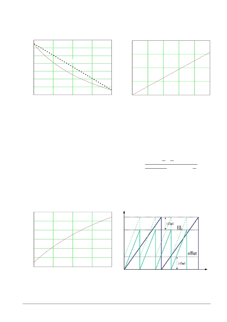
Figure 16. Peak Current Evolution with Input
Voltage in a QR Converter at Constant Output
Power (100 W)
Figure 17. I
P
Evolution with Output Power
3.2
3.1
3.0
2.9
2.8
2.7
2.6
2.5200
250
300
350
400
V
in
, VOLTAGE (V)
P
O
0
20
40
60
80
100
4
3
2
1
0
I
P
I
P
Required I
Pmax
As a result, we will probably calculate our sense resistor
to let the converter bring the peak current up to 3.15 A at low
mains (200 VDC in followerboost configuration).
Unfortunately, in high mains conditions, where the PFC
delivers up to 400 VDC, the controller will also allow the
same 3.15 A maximum peak current (even a little more with
the propagation delay) and the power will dramatically
increase. In these conditions, the maximum power shall
absolutely be clamped in order to avoid lethal runaways in
presence of a fault. If overpower compensation via a resistor
to the bulk capacitor offers a possible way, it suffers from the
lack of precision and good repeatability in production. It also
degrades the standby consumption.
Since our controller integrates a brownout (BO)
protection that permanently senses the bulk capacitor, we
naturally have a voltage image of the bulk voltage. By
converting the BO level into a current, then routing this
current in the current sense (CS) pin, we can easily create a
variable offset that will compensate the maximum output
power. This would result in a variable I
Pmax
as exemplified
by the dashed line on Figure 16.
From the peak current definition, we can extract the output
power variation, with a fixed peak current (the maximum
peak the controller will authorize is 0.8 / R
sense
) and thus
quantify the difference between low and high line:
Pnc(Vin) :
0.8
RS
Vin
LP
tP
2
(
(Vin(Vout
VF)))
Vout
VF
Vin
N
(eq. 4)
where
t
P
is the propagation delay (100 ns typically).
If we enter our previous parameters into the
noncompensated output power definition and plot the result
versus the input voltage, then we obtain the following graph,
Figure 18:
Figure 18. Output Power Evolution with the Input
Voltage (No Compensation)
V
in
, VOLTAGE (V)
I
P
130
125
120
115
110
105
100
200
250
300
350
400
Figure 19. A Possible Way to Compensate the
Current Excursion Lies in Offsetting the
Current Floor
0.8 V
0.64 V
t
I
P
LL
相關PDF資料 |
PDF描述 |
|---|---|
| NCP1395APG | High Performance Resonant Mode Controller |
| NCP1395ADR2G | High Performance Resonant Mode Controller |
| NCP1395BDR2G | High Performance Resonant Mode Controller |
| NCP1395BPG | High Performance Resonant Mode Controller |
| NCP1395A | High Performance Resonant Mode Controller(高性能諧振模式控制器) |
相關代理商/技術參數 |
參數描述 |
|---|---|
| NCP1382DR2G | 功能描述:電流型 PWM 控制器 L-STNDBY PWM CNTRLR RoHS:否 制造商:Texas Instruments 開關頻率:27 KHz 上升時間: 下降時間: 工作電源電壓:6 V to 15 V 工作電源電流:1.5 mA 輸出端數量:1 最大工作溫度:+ 105 C 安裝風格:SMD/SMT 封裝 / 箱體:TSSOP-14 |
| NCP1392B | 制造商:ONSEMI 制造商全稱:ON Semiconductor 功能描述:High-Voltage Half-Bridge Driver with Inbuilt Oscillator |
| NCP1392B_09 | 制造商:ONSEMI 制造商全稱:ON Semiconductor 功能描述:High-Voltage Half-Bridge Driver with Inbuiltc Oscillator |
| NCP1392BDR2G | 功能描述:功率驅動器IC HV HALF-BRIDGE DRVER RoHS:否 制造商:Micrel 產品:MOSFET Gate Drivers 類型:Low Cost High or Low Side MOSFET Driver 上升時間: 下降時間: 電源電壓-最大:30 V 電源電壓-最小:2.75 V 電源電流: 最大功率耗散: 最大工作溫度:+ 85 C 安裝風格:SMD/SMT 封裝 / 箱體:SOIC-8 封裝:Tube |
| NCP1392DDR2G | 功能描述:功率驅動器IC HV HALF-BRIDGE DRIVER RoHS:否 制造商:Micrel 產品:MOSFET Gate Drivers 類型:Low Cost High or Low Side MOSFET Driver 上升時間: 下降時間: 電源電壓-最大:30 V 電源電壓-最小:2.75 V 電源電流: 最大功率耗散: 最大工作溫度:+ 85 C 安裝風格:SMD/SMT 封裝 / 箱體:SOIC-8 封裝:Tube |
發布緊急采購,3分鐘左右您將得到回復。