- 您現在的位置:買賣IC網 > PDF目錄361091 > NCP1381DR2G (ON SEMICONDUCTOR) Low−Standby High Performance PWM Controller PDF資料下載
參數資料
| 型號: | NCP1381DR2G |
| 廠商: | ON SEMICONDUCTOR |
| 元件分類: | 穩(wěn)壓器 |
| 英文描述: | Low−Standby High Performance PWM Controller |
| 中文描述: | 1 A SWITCHING CONTROLLER, 125 kHz SWITCHING FREQ-MAX, PDSO14 |
| 封裝: | LEAD FREE, SOIC-14 |
| 文件頁數: | 19/26頁 |
| 文件大小: | 559K |
| 代理商: | NCP1381DR2G |
NCP1381
http://onsemi.com
19
During the startup sequence, the converter starts by itself,
the PFC is in off mode (SW switch is open). However, when
the I
P
Flag is down, without delay, the PFC is turned on. In
shortcircuit mode, the I
P
Flag is constantly high during
startup attempts and the PFC never turns on. This option
reduces the stress on all the elements. The PFC is also in off
mode when in presence of a brownout detection.
In brownout conditions, the PFC is turnedoff. When the
level on Pin 2 is back to normal conditions, then a clean
startup sequence takes place as Figure 28 depicts and the
PFC turns on after the I
P
Flag release. The bullets below
summarize what we have described:
1. On startup, the PFC is turned on immediately after
the I
P
Flag has disappeared (converter is
stabilized). There is no delay.
2. If a shortcircuit occurs, a delay takes place before
shutting off the driving pulses. When the delay is
elapsed, pulses are turned off and the PFC goes in
the off mode. The controller starts to hiccup.
3. In shortcircuit hiccup mode, as I
P
Flag always
stays high (in shortcircuit, there is no FB signal),
the PFC is never activated.
4. if a VCC
OFF
condition occurs, all pulses are
immediately shutdown and the PFC V
CC
goes low
as well.
5. if a brownout condition is sensed, all pulses are
immediately shut down and the PFC V
CC
goes low
as well.
The freedom is given to the designer to use an other signal
than the FB to detect the standby mode and shutdown the
PFC (the voltage from the auxiliary winding, or the average
of the DRV signal for instance).
BrownOut Protection
Also called “Bulk OK” signal (B
OK
), the brownout (BO)
protection prevents the power supply from being adversely
destroyed in case the mains drops to a very low value. When
this occurs, the controller no longer pulses and waits until
the bulk voltage goes back to its normal level. A certain
amount of hysteresis needs to be provided since the bulk
capacitor is affected by some ripple, especially at low input
levels. For that reason, when the BO comparator toggles, the
internal reference voltage changes from 500 mV to 250 mV.
This effect is not latched: that is to say, when the bulk
capacitor is below the target, the controller does not deliver
pulses. As soon as the input voltage growsup and reaches
the level imposed by the resistive divider, pulses are passed
to the internal driver and activate the MOSFET. Figure 29
offers a way to connect the elements around Pin 2 to create
a brownout detection. Please note that this technique does
not use a current source for the hysteresis but rather a
capacitor. It offers a way to freely select the resistive bridge
impedance.
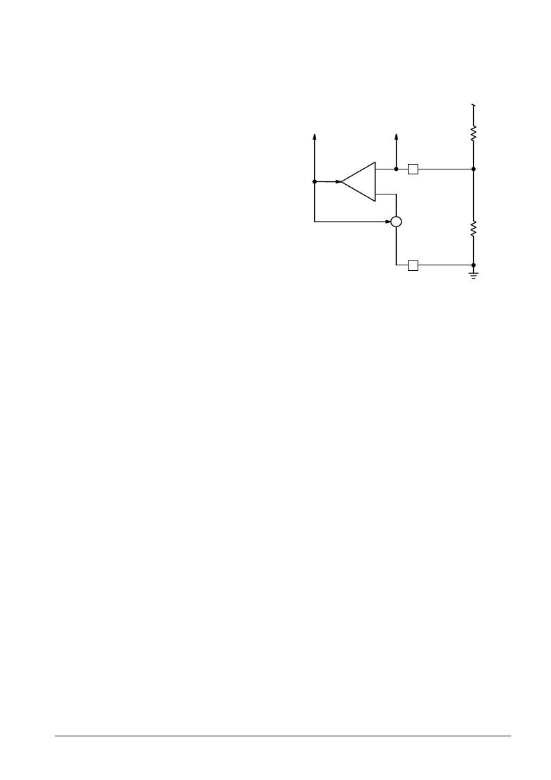
Figure 29. A Way to Implement a BOK Detector
on Pin 2
+
R
lower
250 mV/
500 mV
HV
+
BOK
R
upper
OPP
2
8
The calculation procedure for R
upper
and R
lower
requires
a few lines of algebra. In this configuration, the first level
transition is always clean: the SMPS is not working during
the startup sequence and no ripple exists superimposed on
C
bulk
. Supposed we want to start the operation at
V
bulk
= V
trip
= 120 VDC (V
inAC
= 85 V).
1. Fix a Bridge Current I
b
Compatible with Your
standby Requirements, for Instance an I
b
of 50 A
2. Then Evaluate R
lower
by: R
lower
= 0.5 / I
b
= 10 k
3. Calculate R
upper
by:
(V
trip
0.5 V) / I
b
= (120 0.5) / 50 = 2.39 M
The second threshold, the level at which the power supply
stops (V
stop
), depends on the capacitor C
fil
but also on the
selected bulk capacitor. Furthermore, when the load varies,
the ripple also does and increases as V
in
drops. If C
fil
allows
too much ripple, then chances exist to prematurely stop the
converter. By increasing C
fil
, you have the ability to select
the amount of hysteresis you want to apply. The less ripple
appears on Pin 2, the larger the gap between V
trip
and V
stop
(the maximum being V
stop
= V
trip
/ 2). The best way to assess
the right value of C
fil
, is to use a simple simulation sketch as
the one depicted by Figure 30. A behavioral source loads the
rectified DC line and adjusts itself to draw a given amount
of power, actually the power of your converter (35 W in our
example). The equation associated to B
load
instructs the
simulator to not draw current until the brownout converter
gives the order, just like what the real converter will do. As
a result, V
bulk
is free of ripple until the node CMP goes high,
giving the green light to switch pulses. The input line is
modulated by the “timing” node which ramps up and down
to simulate a slow startup / turnoff sequence. Then, by
adjusting the C
fil
value, it becomes possible to select the
right turn off AC voltage. Figure 31 portrays the typical
signal you can expect from the simulator. We measured a
turn on voltage of 85 VAC whereas the turnoff voltage is
72 VAC. Further increasing C
fil
lowers this level (e.g. a 1 F
gives 65 VAC in the example).
相關PDF資料 |
PDF描述 |
|---|---|
| NCP1395APG | High Performance Resonant Mode Controller |
| NCP1395ADR2G | High Performance Resonant Mode Controller |
| NCP1395BDR2G | High Performance Resonant Mode Controller |
| NCP1395BPG | High Performance Resonant Mode Controller |
| NCP1395A | High Performance Resonant Mode Controller(高性能諧振模式控制器) |
相關代理商/技術參數 |
參數描述 |
|---|---|
| NCP1382DR2G | 功能描述:電流型 PWM 控制器 L-STNDBY PWM CNTRLR RoHS:否 制造商:Texas Instruments 開關頻率:27 KHz 上升時間: 下降時間: 工作電源電壓:6 V to 15 V 工作電源電流:1.5 mA 輸出端數量:1 最大工作溫度:+ 105 C 安裝風格:SMD/SMT 封裝 / 箱體:TSSOP-14 |
| NCP1392B | 制造商:ONSEMI 制造商全稱:ON Semiconductor 功能描述:High-Voltage Half-Bridge Driver with Inbuilt Oscillator |
| NCP1392B_09 | 制造商:ONSEMI 制造商全稱:ON Semiconductor 功能描述:High-Voltage Half-Bridge Driver with Inbuiltc Oscillator |
| NCP1392BDR2G | 功能描述:功率驅動器IC HV HALF-BRIDGE DRVER RoHS:否 制造商:Micrel 產品:MOSFET Gate Drivers 類型:Low Cost High or Low Side MOSFET Driver 上升時間: 下降時間: 電源電壓-最大:30 V 電源電壓-最小:2.75 V 電源電流: 最大功率耗散: 最大工作溫度:+ 85 C 安裝風格:SMD/SMT 封裝 / 箱體:SOIC-8 封裝:Tube |
| NCP1392DDR2G | 功能描述:功率驅動器IC HV HALF-BRIDGE DRIVER RoHS:否 制造商:Micrel 產品:MOSFET Gate Drivers 類型:Low Cost High or Low Side MOSFET Driver 上升時間: 下降時間: 電源電壓-最大:30 V 電源電壓-最小:2.75 V 電源電流: 最大功率耗散: 最大工作溫度:+ 85 C 安裝風格:SMD/SMT 封裝 / 箱體:SOIC-8 封裝:Tube |
發(fā)布緊急采購,3分鐘左右您將得到回復。