- 您現在的位置:買賣IC網 > PDF目錄382369 > P87LPC760 (NXP Semiconductors N.V.) Low power, low price, low pin count (14 pin) microcontroller with 1 kbyte OTP PDF資料下載
參數資料
| 型號: | P87LPC760 |
| 廠商: | NXP Semiconductors N.V. |
| 英文描述: | Low power, low price, low pin count (14 pin) microcontroller with 1 kbyte OTP |
| 中文描述: | 低功耗,低價格,低引腳數(14針),1字節檢察官辦公室微控制器 |
| 文件頁數: | 49/56頁 |
| 文件大小: | 290K |
| 代理商: | P87LPC760 |
第1頁第2頁第3頁第4頁第5頁第6頁第7頁第8頁第9頁第10頁第11頁第12頁第13頁第14頁第15頁第16頁第17頁第18頁第19頁第20頁第21頁第22頁第23頁第24頁第25頁第26頁第27頁第28頁第29頁第30頁第31頁第32頁第33頁第34頁第35頁第36頁第37頁第38頁第39頁第40頁第41頁第42頁第43頁第44頁第45頁第46頁第47頁第48頁當前第49頁第50頁第51頁第52頁第53頁第54頁第55頁第56頁
Philips Semiconductors
Preliminary data
P87LPC760
Low power, low price, low pin count (14 pin)
microcontroller with 1 kbyte OTP
2002 Mar 07
46
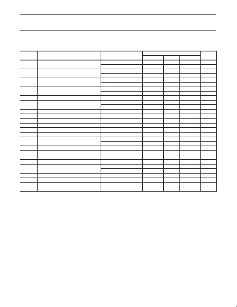
DC ELECTRICAL CHARACTERISTICS
V
DD
= 2.7 V to 6.0 V unless otherwise specified; T
amb
= 0
°
C to +70
°
C, unless otherwise specified.
SYMBOL
PARAMETER
TEST CONDITIONS
LIMITS
TYP
1,2
15
4
4
2
6
2
1
1
–
–
–
–
–
–
0.2 V
DD
–
–
–
–
–
–
–
–
–
–
–
–
–
1.26
UNIT
MIN
–
–
–
–
–
–
–
–
1.5
–0.5
–0.5
–0.5
MAX
25
7
–
–
10
4
10
5
–
I
DD
Power supply current operating
ly current, o erating
5.0 V, 20 MHz
11
3.0 V, 10 MHz
11
5.0 V, 6 MHz
11
3.0 V, 6 MHz
11
5.0 V, 20 MHz
11
3.0 V, 10 MHz
11
5.0 V
11
3.0 V
11
mA
mA
mA
mA
mA
mA
μ
A
μ
A
V
V
V
V
V
V
V
V
V
V
V
V
pF
μ
A
μ
A
μ
A
μ
A
k
V
V
V
I
RC
Power supply current, o erating RC Osc.
I
ID
Power supply current Idle mode
ly current, Idle mode
I
PD
Power supply current Power Down mode
ly current, Power Down mode
V
RAM
RAM keep-alive voltage
V
IL
Input low voltage (TTL input)
In ut low voltage (TTL in ut)
4.0 V < V
DD
< 6.0 V
2.7 V < V
DD
< 4.0 V
0.2 V
DD
–0.1
0.7
0.3 V
DD
V
DD
+0.5
V
DD
+0.5
–
0.4
1.0
–
–
–
15
–50
±
2
–250
–650
225
2.69
3.99
1.41
V
IL1
V
IH
V
IH1
HYS
V
OL
V
OL1
Negative going threshold (Schmitt input)
Input high voltage (TTL input)
Positive going threshold (Schmitt input)
Hysteresis voltage
Output low voltage all ports
5, 9
Output low voltage all ports
5, 9
0.2 V
DD
+0.9
0.7V
DD
–
–
–
V
DD
–0.7
V
DD
–0.7
V
DD
–0.7
–
–
–
–30
–150
40
2.35
3.45
1.11
I
OL
= 3.2 mA, V
DD
= 2.7 V
I
OL
= 20 mA, V
DD
= 2.7 V
I
OH
= –20
μ
A, V
DD
= 2.7 V
I
OH
= –30
μ
A, V
DD
= 4.5 V
I
OH
= –1.0 mA, V
DD
= 2.7 V
V
OH
Output high voltage all ports
Out ut high voltage, all orts
3
V
OH1
C
IO
I
IL
I
LI
Output high voltage, all ports
4
Input/Output pin capacitance
10
Logical 0 input current, all ports
8
Input leakage current, all ports
7
V
IN
= 0.4 V
V
IN
= V
IL
or V
IH
V
IN
= 1.5 V at V
DD
= 3.0 V
V
IN
= 2.0 V at V
DD
= 5.5 V
I
TL
Logical 1 to 0 transition current all ports
Logical 1 to 0 transition current, all orts
3, 6
R
RST
V
BOLOW
V
BOHI
V
REF
NOTES:
1. Typical ratings are not guaranteed. The values listed are at room temperature, 5 V.
2. See other Figures for details.
3. Ports in quasi-bidirectional mode with weak pull-up (applies to all port pins with pull-ups). Does not apply to open drain pins.
4. Ports in PUSH-PULL mode. Does not apply to open drain pins.
5. In all output modes except high impedance mode.
6. Port pins source a transition current when used in quasi-bidirectional mode and externally driven from 1 to 0. This current is highest when
V
IN
is approximately 2 V.
7. Measured with port in high impedance mode. Parameter is guaranteed but not tested at cold temperature.
8. Measured with port in quasi-bidirectional mode.
9. Under steady state (non-transient) conditions, I
OL
must be externally limited as follows:
Maximum I
per port pin:
20 mA
Maximum total I
OL
for all outputs:
80 mA
Maximum total I
for all outputs:
5 mA
If I
OL
exceeds the test condition, V
OL
may exceed the related specification. Pins are not guaranteed to sink current greater than the listed
test conditions.
10.Pin capacitance is characterized but not tested.
11. The I
, I
, and I
specifications are measured using an external clock with the following functions disabled: comparators, brownout
detect, and watchdog timer. For V
= 3 V, LPEP = 1. Refer to the appropriate figures on the following pages for additional current drawn by
each of these functions and detailed graphs for other frequency and voltage combinations.
12.Devices initially operating at V
DD
= 2.7 V or above, and at f
OSC
= 10 MHz or less, are guaranteed to continue to execute instructions
correctly at the brownout trip point. Initial power-on operation below V
DD
= 2.7 V is not guaranteed.
13.Devices initially operating at V
DD
= 4.0 V or above and at f
OSC
= 20 MHz or less are guaranteed to continue to execute instructions correctly
at the brownout trip point. Initial power-on operation below V
DD
= 4.0 V and f
OSC
> 10 MHz is not guaranteed.
Internal reset pull-up resistor
Brownout trip voltage with BOV = 1
12
Brownout trip voltage with BOV = 0
Reference voltage
相關PDF資料 |
PDF描述 |
|---|---|
| P87LPC761 | Low power, low price, low pin count (16 pin) microcontroller with 2 kbyte OTP |
| P87LPC762 | Low power, low price, low pin count 20 pin microcontroller with 2 kbyte OTP |
| P87LPC768 | Low Power, Low System Cost 80C51 MCU with ADC and PWM |
| P87LPC768BN | Low Power, Low System Cost 80C51 MCU with ADC and PWM |
| P88-3004 | TONER VACUUM STD 220/240V |
相關代理商/技術參數 |
參數描述 |
|---|---|
| P87LPC760BDH | 功能描述:8位微控制器 -MCU 80C51 1K/128 OTP RoHS:否 制造商:Silicon Labs 核心:8051 處理器系列:C8051F39x 數據總線寬度:8 bit 最大時鐘頻率:50 MHz 程序存儲器大小:16 KB 數據 RAM 大小:1 KB 片上 ADC:Yes 工作電源電壓:1.8 V to 3.6 V 工作溫度范圍:- 40 C to + 105 C 封裝 / 箱體:QFN-20 安裝風格:SMD/SMT |
| P87LPC760BDH,112 | 功能描述:8位微控制器 -MCU 80C51 1K/128 OTP RoHS:否 制造商:Silicon Labs 核心:8051 處理器系列:C8051F39x 數據總線寬度:8 bit 最大時鐘頻率:50 MHz 程序存儲器大小:16 KB 數據 RAM 大小:1 KB 片上 ADC:Yes 工作電源電壓:1.8 V to 3.6 V 工作溫度范圍:- 40 C to + 105 C 封裝 / 箱體:QFN-20 安裝風格:SMD/SMT |
| P87LPC760BDH,118 | 功能描述:8位微控制器 -MCU 14 PIN MCU 1KBYTE OTP RoHS:否 制造商:Silicon Labs 核心:8051 處理器系列:C8051F39x 數據總線寬度:8 bit 最大時鐘頻率:50 MHz 程序存儲器大小:16 KB 數據 RAM 大小:1 KB 片上 ADC:Yes 工作電源電壓:1.8 V to 3.6 V 工作溫度范圍:- 40 C to + 105 C 封裝 / 箱體:QFN-20 安裝風格:SMD/SMT |
| P87LPC760BN | 功能描述:8位微控制器 -MCU 1K/128 OTP 2.7-6V COMM DIP RoHS:否 制造商:Silicon Labs 核心:8051 處理器系列:C8051F39x 數據總線寬度:8 bit 最大時鐘頻率:50 MHz 程序存儲器大小:16 KB 數據 RAM 大小:1 KB 片上 ADC:Yes 工作電源電壓:1.8 V to 3.6 V 工作溫度范圍:- 40 C to + 105 C 封裝 / 箱體:QFN-20 安裝風格:SMD/SMT |
| P87LPC760BN,112 | 功能描述:8位微控制器 -MCU 1K/128 OTP 2.7-6V RoHS:否 制造商:Silicon Labs 核心:8051 處理器系列:C8051F39x 數據總線寬度:8 bit 最大時鐘頻率:50 MHz 程序存儲器大小:16 KB 數據 RAM 大小:1 KB 片上 ADC:Yes 工作電源電壓:1.8 V to 3.6 V 工作溫度范圍:- 40 C to + 105 C 封裝 / 箱體:QFN-20 安裝風格:SMD/SMT |
發布緊急采購,3分鐘左右您將得到回復。