- 您現在的位置:買賣IC網 > Datasheet目錄46 > SC403MLTRT (Semtech)IC REG DL BCK/LINEAR SYNC 32MLPQ Datasheet資料下載
參數資料
| 型號: | SC403MLTRT |
| 廠商: | Semtech |
| 文件頁數: | 22/32頁 |
| 文件大小: | 741K |
| 描述: | IC REG DL BCK/LINEAR SYNC 32MLPQ |
| 標準包裝: | 1 |
| 系列: | EcoSpeed®, SmartDrive™ |
| 拓撲: | 降壓(降壓)同步(1),線性(LDO)(1) |
| 功能: | 任何功能 |
| 輸出數: | 2 |
| 頻率 - 開關: | 1MHz |
| 電壓/電流 - 輸出 1: | 可調至 0.75V,6A |
| 電壓/電流 - 輸出 2: | 可調至 0.75V,200mA |
| 帶 LED 驅動器: | 無 |
| 帶監控器: | 無 |
| 帶序列發生器: | 是 |
| 電源電壓: | 3 V ~ 28 V |
| 工作溫度: | -40°C ~ 85°C |
| 安裝類型: | 表面貼裝 |
| 封裝/外殼: | 32-VFQFN 裸露焊盤 |
| 供應商設備封裝: | 32-MLPQ(5x5) |
| 包裝: | 標準包裝 |
| 其它名稱: | SC403MLDKR |
第1頁第2頁第3頁第4頁第5頁第6頁第7頁第8頁第9頁第10頁第11頁第12頁第13頁第14頁第15頁第16頁第17頁第18頁第19頁第20頁第21頁當前第22頁第23頁第24頁第25頁第26頁第27頁第28頁第29頁第30頁第31頁第32頁
SC403
22
Applications Information (continued)
In many applications, the EN/PSV pin will be pulled high to
the VDD node to allow control of the PWM and LDO ENL
pin. If the switch over feature is used, this circuit must be
implemented with caution or the circuit may be damaged.
In the case where the ENL pin is being controlled by a GPIO
signal or is tied directly to the input voltage, the ENL pin can
be pulled low while the PWM is still generating an output
voltage that is seen across one of the switch-over diodes.
This may result in the VDD node being held above its UVLO
threshold while the LDO is deactivated. Operating in this
way can potentially damage the part.
In the case where the ENL pin is used to control the input
UVLO, it is acceptable to connect EN/PSV directly to the
VDD node.
It is not recommended to use the switch-over feature for
an output voltage less than 3V since this does not provide
sufficient voltage for the gate-source drive to the internal
p-channel switch-over MOSFET.
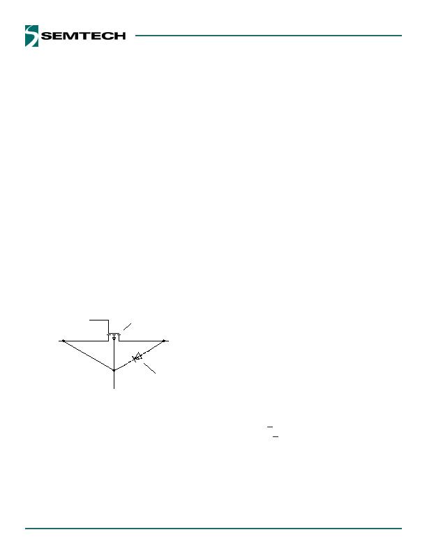
Switch-over MOSFET Parasitic Diode
The switch-over MOSFET contains a parasitic diode that is
inherent to its construction, as shown in Figure 12.
Switchover
MOSFET
Parasitic diode
VDD
LDO
V
OUT
Switchover
control
Figure 12 Switch-over MOSFET Parasitic Diodes
If V
OUT
is higher than VDD, then the diode will turn on and
the SC403 operating current will flow through this diode.
This has the potential of damaging the device.
There are some important design rules that must be fol-
lowed to prevent forward bias of this diode. The following
condition, V
DD
e V
OUT
needs to be satisfied in order for the
parasitic diode to stay off and prevent damaging the
device. Many applications connect the EN pin to V5V and
control the on/off of the LDO and PWM simultaneously
with the ENL pin. This allows one signal to control both
the bias and power output of the SC403. When V
OUT
> 3.0V
this configuration can cause problems due to the parasitic
diodes in the LDO switchover circuitry. After the V
OUT
>
3.0V PWM output is up and running the switchover diodes
can hold up V5V > UVLO even if the ENL pin is grounded,
turning off the LDO. Operating in this way can potentially
damage the part.
Design Procedure
When designing a switch mode supply the input voltage
range, load current, switching frequency, and inductor
ripple current must be specified.
The maximum input voltage (V
INMAX
) is the highest speci-
fed input voltage. The minimum input voltage ( V
INMIN
) is
determined by the lowest input voltage after evaluating
the voltage drops due to connectors, fuses, switches, and
PCB traces.
The following parameters define the design.
Nominal output voltage (V
OUT
)
Static or DC output tolerance
Transient response
Maximum load current (I
OUT
)
There are two values of load current to evaluate con-
tinuous load current and peak load current. Continuous
load current relates to thermal stresses which drive the
selection of the inductor and input capacitors. Peak load
current determines instantaneous component stresses and
fltering requirements such as inductor saturation, output
capacitors, and design of the current limit circuit.
The following values are used in this design.
V
IN
= 12V + 10%
V
OUT
= 1.5V + 4%
f
SW
= 300kHz
Load = 6A maximum
Frequency Selection
Selection of the switching frequency requires making a
trade-off between the size and cost of the external filter
components (inductor and output capacitor) and the
power conversion efficiency.
"
"
"
"
"
"
"
"
相關PDF資料 |
PDF描述 |
|---|---|
| SC418ULTRT | IC REG DL BUCK/LINEAR 20MLPQ |
| SC424MLTRT | IC REG DL BUCK/LINEAR 28MLPQ |
| SC4250LISTRT | IC HOT SWAP CTRLR 8-SOIC |
| SC427MLTRT | IC REG DL BUCK/LINEAR 32MLPQ |
| SE95D,112 | IC SENSOR TEMP 2.8-5.5V SOT96-1 |
相關代理商/技術參數 |
參數描述 |
|---|---|
| SC4040 | 制造商:SEMTECH 制造商全稱:Semtech Corporation 功能描述:PRECISION SHUNT VOLTAGE REFERENCE |
| SC4040AS | 制造商:SEMTECH 制造商全稱:Semtech Corporation 功能描述:PRECISION SHUNT VOLTAGE REFERENCE |
| SC4040ASK | 制造商:SEMTECH 制造商全稱:Semtech Corporation 功能描述:PRECISION SHUNT VOLTAGE REFERENCE |
| SC4040ASK.TR | 制造商:Semtech Corporation 功能描述:IC V-REF PRECISION 2.5V 3SOT-23 T/R |
| SC4040AZ | 制造商:SEMTECH 制造商全稱:Semtech Corporation 功能描述:PRECISION SHUNT VOLTAGE REFERENCE |
發布緊急采購,3分鐘左右您將得到回復。