- 您現在的位置:買賣IC網 > PDF目錄98215 > TFP401AMPZPEP (TEXAS INSTRUMENTS INC) SPECIALTY CONSUMER CIRCUIT, PQFP100 PDF資料下載
參數資料
| 型號: | TFP401AMPZPEP |
| 廠商: | TEXAS INSTRUMENTS INC |
| 元件分類: | 消費家電 |
| 英文描述: | SPECIALTY CONSUMER CIRCUIT, PQFP100 |
| 封裝: | 14 X 14 MM, 1 MM HEIGHT, 0.50 MM PITCH, GREEN, PLASTIC, HTQFP-100 |
| 文件頁數: | 19/21頁 |
| 文件大小: | 460K |
| 代理商: | TFP401AMPZPEP |
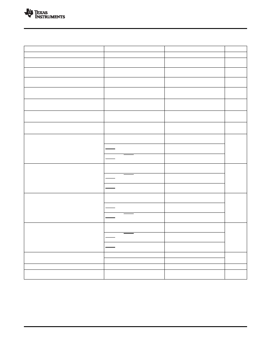
AC ELECTRICAL CHARACTERISTICS
www.ti.com .................................................................................................................................................................................................. SLDS160 – MARCH 2009
over operating free-air temperature range (unless otherwise noted)
PARAMETER
TEST CONDITIONS
MIN
TYP
MAX
UNIT
VID(2)
Differential input sensitivity(1)
150
1560
mVp-p
tps
Analog input intra-pair (+ to -)
0.4
tbit
(3)
differential skew (2)
tccs
Analog Input inter-pair or
1
tpix
(4)
channel-to-channel skew (2)
tijit
Worse case differential input clock
50
ps
jitter tolerance(5), (2)(6)
tf1
Fall time of data and control
ST = Low,
CL=5 pF
2.4
ns
signals(7), (8)(6)
ST = High,
CL=10 pF
1.9
tr1
Rise time of data and control
ST = Low,
CL=5 pF
2.4
ns
signals(7), (8)(6)
ST = High,
CL=10 pF
1.9
tr2
Rise time of ODCK clock(7)(6)
ST = Low,
CL=5 pF
2.4
ns
ST = High,
CL=10 pF
1.9
tf2
Fall time of ODCK clock(7)(6)
ST = Low,
CL=5 pF
2.4
ns
ST = High,
CL=10 pF
1.9
tsu1
Setup time, data and control signal to
1 pixel/clock, PIXS = low,
1.8
falling edge of ODCK(6)
OCK_INV = low
2 pixel/clock, PIXS = high,
3.8
ns
STAG = high, OCK_INV = low
2 pixel and STAG, PIXS = high,
0.6
STAG = low, OCK_INV = low
th1
Hold time, data and control signal to
1 pixel/clock, PIXS = low,
0.6
falling edge of ODCK(6)
OCK_INV = low
2 pixel and STAG, PIXS = high,
2.5
ns
STAG = low, OCK_INV = low
2 pixel/clock, PIXS = high,
2.9
STAG = high, OCK_INV = low
tsu2
Setup time, data and control signal to
1 pixel/clock, PIXS = low,
2.1
rising edge of ODCK(6)
OCK_INV = high
2 pixel/clock, PIXS = high,
4
ns
STAG = high, OCK_INV = high
2 pixel and STAG, PIXS = high,
1.5
STAG = low, OCK_INV = high
th2
Hold time, data and control signal to
1 pixel/clock, PIXS = low,
0.3
rising edge of ODCK(6)
OCK_INV = high
2 pixel and STAG, PIXS = high,
2.4
ns
STAG = low, OCK_INV = high
2 pixel/clock, PIXS = high,
2.1
STAG = high, OCK_INV = high
fODCK
ODCK frequency
PIX = Low (1-PIX/CLK)
25
165
MHz
PIX = High (2-PIX/CLK)
12.5
82.5
ODCK duty-cycle
45%
60%
75%
tpd(PDL)
Propagation delay time from PD low
9
ns
to Hi-Z outputs(6)
(1)
Specified as ac parameter to include sensitivity to overshoot, undershoot and reflection.
(2)
By characterization
(3)
tbit is 1/10 the pixel time, tpix
(4)
tpix is the pixel time defined as the period of the RxC input clock. The period of ODCK is equal to tpix in 1-pixel/clock mode or 2tpix when
in 2-pixel/clock mode.
(5)
Measured differentially at 50% crossing using ODCK output clock as trigger.
(6)
Not Production Test
(7)
Rise and fall times measured as time between 20% and 80% of signal amplitude.
(8)
Data and control signals are : QE[23:0], QO[23:0], DE, HSYNC, VSYNC and CTL[3:1]
Copyright 2009, Texas Instruments Incorporated
7
Product Folder Link(s): TFP401A-EP
相關PDF資料 |
PDF描述 |
|---|---|
| TFP401APZP | SPECIALTY CONSUMER CIRCUIT, PQFP100 |
| TFP401APZPG4 | SPECIALTY CONSUMER CIRCUIT, PQFP100 |
| TFP401PZP | SPECIALTY CONSUMER CIRCUIT, PQFP100 |
| TFP401PZPG4 | SPECIALTY CONSUMER CIRCUIT, PQFP100 |
| TFP403PZP | SPECIALTY CONSUMER CIRCUIT, PQFP100 |
相關代理商/技術參數 |
參數描述 |
|---|---|
| TFP401APZP | 功能描述:顯示接口集成電路 PanelBus DVI Rcvr 165MHz HSYNC fix RoHS:否 制造商:Texas Instruments 電源電流:125 mA 工作溫度范圍:- 40 C to + 105 C 封裝 / 箱體:WQFN-60 封裝:Reel |
| TFP401APZPG4 | 功能描述:顯示接口集成電路 PanelBus DVI Rcvr RoHS:否 制造商:Texas Instruments 電源電流:125 mA 工作溫度范圍:- 40 C to + 105 C 封裝 / 箱體:WQFN-60 封裝:Reel |
| TFP401PZP | 功能描述:顯示接口集成電路 PanelBus DVI Receiver 165MHz RoHS:否 制造商:Texas Instruments 電源電流:125 mA 工作溫度范圍:- 40 C to + 105 C 封裝 / 箱體:WQFN-60 封裝:Reel |
| TFP401PZPG4 | 功能描述:顯示接口集成電路 PanelBus DVI Rcvr RoHS:否 制造商:Texas Instruments 電源電流:125 mA 工作溫度范圍:- 40 C to + 105 C 封裝 / 箱體:WQFN-60 封裝:Reel |
| TFP403 | 制造商:TI 制造商全稱:Texas Instruments 功能描述:TI PANEBUS DIGITAL RECEIVER |
發布緊急采購,3分鐘左右您將得到回復。