- 您現(xiàn)在的位置:買(mǎi)賣(mài)IC網(wǎng) > PDF目錄98266 > TMC2491AR2C (FAIRCHILD SEMICONDUCTOR CORP) COLOR SIGNAL ENCODER, PQCC44 PDF資料下載
參數(shù)資料
| 型號(hào): | TMC2491AR2C |
| 廠商: | FAIRCHILD SEMICONDUCTOR CORP |
| 元件分類(lèi): | 顏色信號(hào)轉(zhuǎn)換 |
| 英文描述: | COLOR SIGNAL ENCODER, PQCC44 |
| 封裝: | PLASTIC, LCC-44 |
| 文件頁(yè)數(shù): | 12/36頁(yè) |
| 文件大小: | 208K |
| 代理商: | TMC2491AR2C |
第1頁(yè)第2頁(yè)第3頁(yè)第4頁(yè)第5頁(yè)第6頁(yè)第7頁(yè)第8頁(yè)第9頁(yè)第10頁(yè)第11頁(yè)當(dāng)前第12頁(yè)第13頁(yè)第14頁(yè)第15頁(yè)第16頁(yè)第17頁(yè)第18頁(yè)第19頁(yè)第20頁(yè)第21頁(yè)第22頁(yè)第23頁(yè)第24頁(yè)第25頁(yè)第26頁(yè)第27頁(yè)第28頁(yè)第29頁(yè)第30頁(yè)第31頁(yè)第32頁(yè)第33頁(yè)第34頁(yè)第35頁(yè)第36頁(yè)
TMC2490A/TMC2491A
PRODUCT SPECIFICATION
2
Functional Description
The TMC2490(1)A is a fully-integrated digital video
encoder with simultaneous composite and Y/C (S-Video)
outputs, compatible with NTSC, NTSC-EIA, and all PAL
television standards.
Digital component video is accepted at the PD port in 8-bit
parallel CCIR-601/656 format. It is demultiplexed into
luminance and chrominance components. The chrominance
components modulate a digitally synthesized subcarrier.
The luminance and chrominance signals are then separately
interpolated to twice the input pixel rate and converted to
analog signals by 10-bit D/A converters. They are also
digitally combined and the resulting composite signal is
output by a third 10-bit D/A converter.
The TMC2490(1)A operates from a single clock at 27 MHz,
twice the system pixel rate. Programmable control registers
allow software control of subcarrier frequency and phase
parameters. Incoming YCBCR422 digital video is interpo-
lated to YCBCR444 format for encoding.
Internal control registers can be accessed over a standard
8-bit parallel microprocessor port or a 2-pin (clock and data)
serial port.
Sync Generator
The TMC2490(1)A operates in master or slave mode. In
slave mode, it extracts its horizontal and vertical sync timing
and eld information from the CCIR-656 SAV (Start of
Active Video) and EAV (End of Active Video) signal in the
incoming data stream. In master mode, it generates a
13.5 MHz timebase and sends line and eld synchronizing
signals to the host system.
Horizontal and vertical synchronization pulses in the analog
output are digitally generated by the TMC2490(1)A with
controlled rise and fall times on all sync edges, the beginning
and end of active video, and the burst envelope.
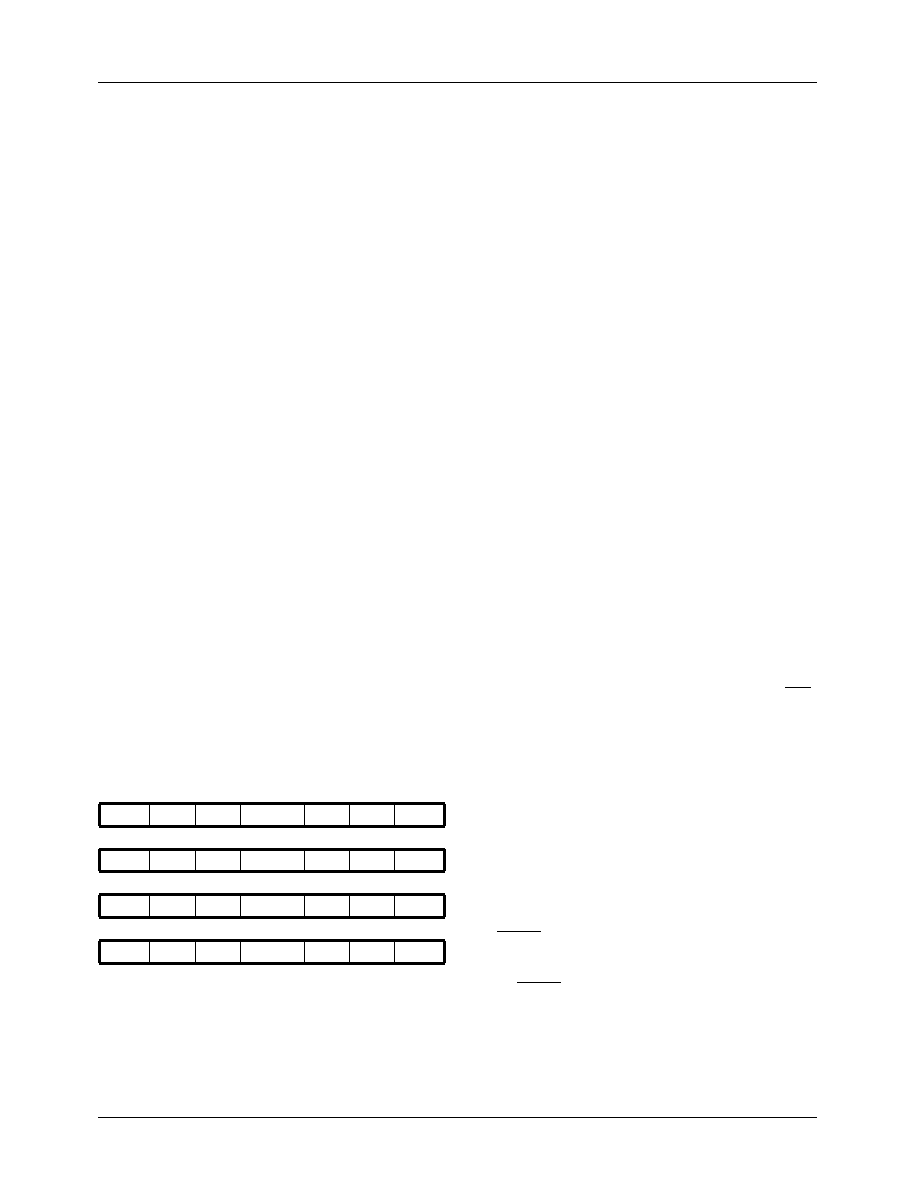
Figure 1. Pixel Data Format
Chroma Modulator
A digital subcarrier synthesizer generates the reference for
a quadrature modulator, producing a digital chrominance
signal. The chroma bandwidth may be programmed to
650 kHz or 1.3 MHz.
Interpolation Filters
Interpolation lters on the luminance and chrominance
signals double the pixel rate to 27Mpps before D/A conver-
sion. This low-pass ltering and oversampling process
reduces sin(x)/x roll-off, and greatly simplies the analog
reconstruction lter required after the D/A converters.
D/A Converters
Analog outputs of the TMC2490(1)A are driven by three 10-
bit D/A converters, The outputs drive standard video levels
into 37.5 or 75 Ohm loads. An internal voltage reference is
used to provide reference current for the D/A converters. An
external xed or variable voltage reference source can also
be used. The video signal levels from the TMC2490(1)A
may be adjusted to overcome the insertion loss of analog
low-pass output lters by varying RREF or VREF.
Macrovision 7.01
To deter unauthorized video taping, the output data stream
can be modied per the Macrovision antitaping process
(Revision 7.01). The TMC2491A data sheet supplement con-
tains information on the application of Macrovision antitap-
ing process (Revision 7.01). Only Macrovision licensees will
be able to receive this information.
Parallel and Serial Microprocessor Interfaces
The parallel microprocessor interface employs 11 pins.
These are shared with the serial interface. A single pin, SER,
selects between the two interface modes.
In parallel interface mode, one address pin is decoded to
enable access to the internal control register and its pointer.
Controls are reached by loading a desired address through
the 8-bit D7-0 port, followed by the desired data (read or
write) for that address. The control register address pointer
auto-increments to address 22h and then remains there.
A 2-line serial interface is also provided on the
TMC2490(1)A for initialization and control. The same set of
registers accessed by the parallel port is available to the
serial port.
The RESET pin sets all internal state machines and control
registers to their initialized conditions, disables the analog
outputs, and places the encoder in a reset mode. At the rising
edge of RESET, the encoder is automatically initialized in
NTSC-M format.
MSB
LSB
PD7
CB (n)
PD0
PD7
Y (n)
PD0
PD7
CR (n)
PD0
PD7
Y (n+1)
PD0
相關(guān)PDF資料 |
PDF描述 |
|---|---|
| TMC2491R2C | COLOR SIGNAL ENCODER, PQCC44 |
| TMC2493R2C | COLOR SIGNAL ENCODER, PQCC44 |
| TMC2590R2C | COLOR SIGNAL ENCODER, PQCC44 |
| TMC2601R2C | SPECIALTY CONSUMER CIRCUIT, PQCC44 |
| TMC3003KR2C30 | TRIPLE, PARALLEL, WORD INPUT LOADING, 0.015 us SETTLING TIME, 10-BIT DAC, PQFP48 |
相關(guān)代理商/技術(shù)參數(shù) |
參數(shù)描述 |
|---|---|
| TMC249A | 制造商:未知廠家 制造商全稱:未知廠家 功能描述:High Current Microstep Stepper Motor Driver with sensorless stall detection, protection / diagnostics and SPI Interface |
| TMC249-A | 制造商:未知廠家 制造商全稱:未知廠家 功能描述:High Current Microstep Stepper Motor Driver with Sensorless Stall D e t e c t i o n ,P rotection / Diagnosis and SPI Interface |
| TMC249A-LA | 制造商:Trinamic 功能描述:IC BRIDGE DRIVER SPI/ANLG 32QFN |
| TMC249A-SA | 制造商:Trinamic 功能描述:STEPPER MOTOR DRIVER SMD SO-28 制造商:Trinamic 功能描述:STEPPER MOTOR DRIVER, SMD, SO-28 制造商:Trinamic 功能描述:IC MOTOR DRIVER, FULL BRIDGE, 1mA SOIC-28; Motor Type:Full Bridge; No. of Outputs:8; Output Current:1mA; Output Voltage:34V; Driver Case Style:SOIC; No. of Pins:28; Supply Voltage Min:3V; Supply Voltage Max:5.5V; MSL:MSL 2 - 1 year ;RoHS Compliant: Yes |
| TMC249-EVAL | 制造商:Trinamic 功能描述:EVALUATION BOARD FOR TMC249 |
發(fā)布緊急采購(gòu),3分鐘左右您將得到回復(fù)。