- 您現在的位置:買賣IC網 > PDF目錄21990 > XC2S50-5TQG144C (Xilinx Inc)IC SPARTAN-II FPGA 50K 144-TQFP PDF資料下載
參數資料
| 型號: | XC2S50-5TQG144C |
| 廠商: | Xilinx Inc |
| 文件頁數: | 89/99頁 |
| 文件大小: | 0K |
| 描述: | IC SPARTAN-II FPGA 50K 144-TQFP |
| 標準包裝: | 60 |
| 系列: | Spartan®-II |
| LAB/CLB數: | 384 |
| 邏輯元件/單元數: | 1728 |
| RAM 位總計: | 32768 |
| 輸入/輸出數: | 92 |
| 門數: | 50000 |
| 電源電壓: | 2.375 V ~ 2.625 V |
| 安裝類型: | 表面貼裝 |
| 工作溫度: | 0°C ~ 85°C |
| 封裝/外殼: | 144-LQFP |
| 供應商設備封裝: | 144-TQFP(20x20) |
| 產品目錄頁面: | 599 (CN2011-ZH PDF) |
| 其它名稱: | 122-1321 |
第1頁第2頁第3頁第4頁第5頁第6頁第7頁第8頁第9頁第10頁第11頁第12頁第13頁第14頁第15頁第16頁第17頁第18頁第19頁第20頁第21頁第22頁第23頁第24頁第25頁第26頁第27頁第28頁第29頁第30頁第31頁第32頁第33頁第34頁第35頁第36頁第37頁第38頁第39頁第40頁第41頁第42頁第43頁第44頁第45頁第46頁第47頁第48頁第49頁第50頁第51頁第52頁第53頁第54頁第55頁第56頁第57頁第58頁第59頁第60頁第61頁第62頁第63頁第64頁第65頁第66頁第67頁第68頁第69頁第70頁第71頁第72頁第73頁第74頁第75頁第76頁第77頁第78頁第79頁第80頁第81頁第82頁第83頁第84頁第85頁第86頁第87頁第88頁當前第89頁第90頁第91頁第92頁第93頁第94頁第95頁第96頁第97頁第98頁第99頁
Spartan-II FPGA Family: Functional Description
DS001-2 (v2.8) June 13, 2008
Module 2 of 4
Product Specification
9
R
drivers are disabled. Maintaining a valid logic level in this
way helps eliminate bus chatter.
Because the weak-keeper circuit uses the IOB input buffer
to monitor the input level, an appropriate VREF voltage must
be provided if the signaling standard requires one. The
provision of this voltage must comply with the I/O banking
rules.
I/O Banking
Some of the I/O standards described above require VCCO
and/or VREF voltages. These voltages are externally
connected to device pins that serve groups of IOBs, called
banks. Consequently, restrictions exist about which I/O
standards can be combined within a given bank.
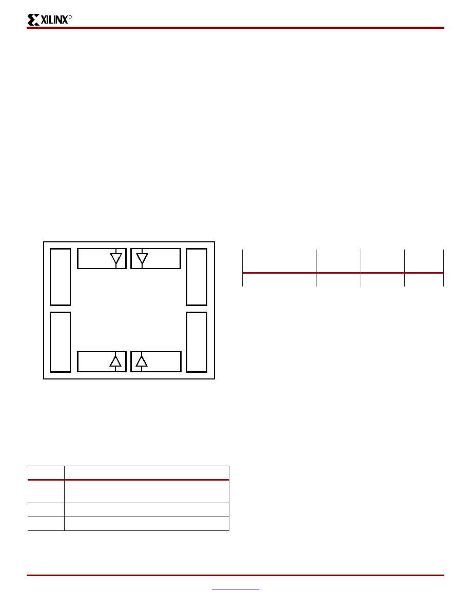
Eight I/O banks result from separating each edge of the
FPGA into two banks (see Figure 3). Each bank has
multiple VCCO pins which must be connected to the same
voltage. Voltage is determined by the output standards in
use.
Within a bank, output standards may be mixed only if they
use the same VCCO. Compatible standards are shown in
Table 4. GTL and GTL+ appear under all voltages because
their open-drain outputs do not depend on VCCO.
Some input standards require a user-supplied threshold
voltage, VREF. In this case, certain user-I/O pins are
automatically configured as inputs for the VREF voltage.
About one in six of the I/O pins in the bank assume this role.
VREF pins within a bank are interconnected internally and
consequently only one VREF voltage can be used within
each bank. All VREF pins in the bank, however, must be
connected to the external voltage source for correct
operation.
In a bank, inputs requiring VREF can be mixed with those
that do not but only one VREF voltage may be used within a
bank. Input buffers that use VREF are not 5V tolerant.
LVTTL, LVCMOS2, and PCI are 5V tolerant. The VCCO and
VREF pins for each bank appear in the device pinout tables.
Within a given package, the number of VREF and VCCO pins
can vary depending on the size of device. In larger devices,
more I/O pins convert to VREF pins. Since these are always
a superset of the VREF pins used for smaller devices, it is
possible to design a PCB that permits migration to a larger
device. All VREF pins for the largest device anticipated must
be connected to the VREF voltage, and not used for I/O.
Configurable Logic Block
The basic building block of the Spartan-II FPGA CLB is the
logic cell (LC). An LC includes a 4-input function generator,
carry logic, and storage element. Output from the function
generator in each LC drives the CLB output and the D input
of the flip-flop. Each Spartan-II FPGA CLB contains four
LCs, organized in two similar slices; a single slice is shown
in Figure 4.
In addition to the four basic LCs, the Spartan-II FPGA CLB
contains logic that combines function generators to provide
functions of five or six inputs.
Look-Up Tables
Spartan-II FPGA function generators are implemented as
4-input look-up tables (LUTs). In addition to operating as a
function generator, each LUT can provide a 16 x 1-bit
synchronous RAM. Furthermore, the two LUTs within a
slice can be combined to create a 16 x 2-bit or 32 x 1-bit
synchronous RAM, or a 16 x 1-bit dual-port synchronous
RAM.
The Spartan-II FPGA LUT can also provide a 16-bit shift
register that is ideal for capturing high-speed or burst-mode
data. This mode can also be used to store data in
applications such as Digital Signal Processing.
Figure 3: Spartan-II I/O Banks
Table 4: Compatible Output Standards
VCCO
Compatible Standards
3.3V
PCI, LVTTL, SSTL3 I, SSTL3 II, CTT, AGP,
GTL, GTL+
2.5V
SSTL2 I, SSTL2 II, LVCMOS2, GTL, GTL+
1.5V
HSTL I, HSTL III, HSTL IV, GTL, GTL+
DS001_03_060100
Bank 0
GCLK3
GCLK2
GCLK1
GCLK0
Bank 1
Bank 5
Bank 4
Spartan-II
Device
Bank
7
Bank
6
Bank
2
Bank
3
Independent Banks Available
Package
VQ100
PQ208
CS144
TQ144
FG256
FG456
Independent Banks
1
4
8
相關PDF資料 |
PDF描述 |
|---|---|
| VI-B6T-CX | CONVERTER MOD DC/DC 6.5V 75W |
| VI-27N-CW-F4 | CONVERTER MOD DC/DC 18.5V 100W |
| DS1631UT/T&R | IC DIGITAL THERM HI PREC 8MSOP |
| VI-B6R-CX | CONVERTER MOD DC/DC 7.5V 75W |
| VI-B6M-CX | CONVERTER MOD DC/DC 10V 75W |
相關代理商/技術參數 |
參數描述 |
|---|---|
| XC2S50-5TQG144I | 制造商:Xilinx 功能描述:FPGA SPARTAN-II 50K GATES 1728 CELLS 263MHZ 2.5V 144TQFP EP - Trays 制造商:Xilinx 功能描述:IC SYSTEM GATE |
| XC2S50-5VQ100C | 制造商:XILINX 制造商全稱:XILINX 功能描述:Spartan-II 2.5V FPGA Family:Introduction and Ordering Information |
| XC2S50-5VQ100I | 制造商:XILINX 制造商全稱:XILINX 功能描述:Spartan-II 2.5V FPGA Family:Introduction and Ordering Information |
| XC2S50-5VQG100C | 制造商:XILINX 制造商全稱:XILINX 功能描述:Spartan-II FPGA Family |
| XC2S50-5VQG100I | 制造商:XILINX 制造商全稱:XILINX 功能描述:Spartan-II FPGA Family |
發布緊急采購,3分鐘左右您將得到回復。