- 您現在的位置:買賣IC網 > PDF目錄373914 > AD7707BR (ANALOG DEVICES INC) 3 V/5 V, +-10 V Input Range, 1 mW 3-Channel 16-Bit, Sigma-Delta ADC PDF資料下載
參數資料
| 型號: | AD7707BR |
| 廠商: | ANALOG DEVICES INC |
| 元件分類: | ADC |
| 英文描述: | 3 V/5 V, +-10 V Input Range, 1 mW 3-Channel 16-Bit, Sigma-Delta ADC |
| 中文描述: | 3-CH 16-BIT DELTA-SIGMA ADC, SERIAL ACCESS, PDSO20 |
| 封裝: | 0.300 INCH, SOIC-20 |
| 文件頁數: | 13/40頁 |
| 文件大小: | 316K |
| 代理商: | AD7707BR |
第1頁第2頁第3頁第4頁第5頁第6頁第7頁第8頁第9頁第10頁第11頁第12頁當前第13頁第14頁第15頁第16頁第17頁第18頁第19頁第20頁第21頁第22頁第23頁第24頁第25頁第26頁第27頁第28頁第29頁第30頁第31頁第32頁第33頁第34頁第35頁第36頁第37頁第38頁第39頁第40頁
REV. A
AD7707
–13–
TEMPERATURE –
8
C
–40
S
m
A
0
4
8
16
20
12
–30 –20 –10
0
10
20
30
40
50
60
70
80
V
DD
= 5V
V
DD
= 3V
MCLK IN = 0V OR V
DD
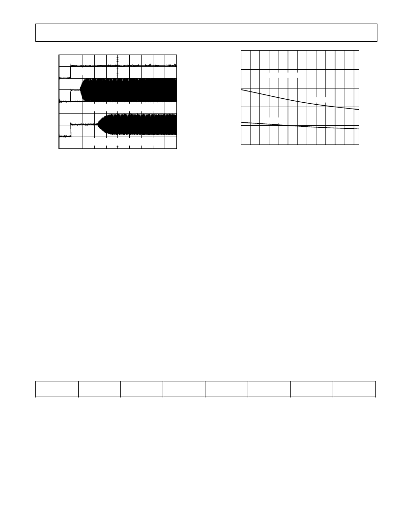
Figure 9. Standby Current vs. Temperature
ON-CHIP REGISTERS
The AD7707 contains eight on-chip registers which can be accessed via the serial port of the part. The first of these is a Communica-
tions Register that controls the channel selection, decides whether the next operation is a read or write operation and also decides
which register the next read or write operation accesses. All communications to the part must start with a write operation to the
Communications Register. After power-on or
RESET
, the device expects a write to its Communications Register. The data written
to this register determines whether the next operation to the part is a read or a write operation and also determines to which register
this read or write operation occurs. Therefore, write access to any of the other registers on the part starts with a write operation to the
Communications Register followed by a write to the selected register. A read operation from any other register on the part (including
the Communications Register itself and the output data register) starts with a write operation to the Communications Register fol-
lowed by a read operation from the selected register. The Communications Register also controls the standby mode and channel
selection and the
DRDY
status is also available by reading from the Communications Register. The second register is a Setup Regis-
ter that determines calibration mode, gain setting, bipolar/unipolar operation and buffered mode. The third register is labelled the
Clock Register and contains the filter selection bits and clock control bits. The fourth register is the Data Register from which the
output data from the part is accessed. The final registers are the calibration registers which store channel calibration data. The regis-
ters are discussed in more detail in the following sections.
Communications Register (RS2, RS1, RS0 = 0, 0, 0)
The Communications Register is an 8-bit register from which data can either be read or to which data can be written. All communi-
cations to the part must start with a write operation to the Communications Register. The data written to the Communications Reg-
ister determines whether the next operation is a read or write operation and to which register this operation takes place. Once the
subsequent read or write operation to the selected register is complete, the interface returns to where it expects a write operation to
the Communications Register. This is the default state of the interface, and on power-up or after a
RESET
, the AD7707 is in this
default state waiting for a write operation to the Communications Register. In situations where the interface sequence is lost, if a
write operation of sufficient duration (containing at least 32 serial clock cycles) takes place with DIN high, the AD7707 returns to
this default state. Table VIII outlines the bit designations for the Communications Register.
Table VIII. Communications Register
0/
DRDY
(0)
RS2 (0)
RS1 (0)
RS0 (0)
R/
W
(0)
STBY (0)
CH1 (0)
CH0 (0)
0/
DRDY
For a write operation, a “0” must be written to this bit so that the write operation to the Communications Register
actually takes place. If a “1” is written to this bit, the part will not clock on to subsequent bits in the register. It will
stay at this bit location until a “0” is written to this bit. Once a “0” is written to this bit, the next seven bits will be
loaded to the Communications Register. For a read operation, this bit provides the status of the
DRDY
flag from
the part. The status of this bit is the same as the
DRDY
output pin.
Register Selection Bits. These three bits select to which one of eight on-chip registers the next read or write opera-
tion takes place, as shown in Table IX, along with the register size. When the read or write operation to the se-
lected register is complete, the part returns to where it is waiting for a write operation to the Communications
Register. It does not remain in a state where it will continue to access the register.
RS2–RS0
CH1 5.00V
CH2 2.00V
2
2
1
TEK STOP: SINGLE SEQ 50.0kS/s
V
DD
OSCILLATOR = 4.9152 MHz
OSCILLATOR = 2.4576 MHz
5ms/DIV
Figure 8. Typical Crystal Oscillator Power-Up Time
相關PDF資料 |
PDF描述 |
|---|---|
| AD7707BRU | 3 V/5 V, +-10 V Input Range, 1 mW 3-Channel 16-Bit, Sigma-Delta ADC |
| AD7707 | ECONOLINE: REC2.2-S_DR/H1 - 2.2W DIP Package- 1kVDC Isolation- Regulated Output- UL94V-0 Package Material- Continuous Short Circiut Protection- Internal SMD design- 100% Burned In- Efficiency to 75% |
| AD7707EB | 3 V/5 V 610 V Input Range 1 mW 3-Channel 16-Bit Sigma-Delta ADC(316.51 k) |
| AD7708BR | Shaft; Style: 2 - light; Applicable Model: LE-P / LEL-W |
| AD7708BRU | 8-/10-Channel, Low Voltage, Low Power, ADCs |
相關代理商/技術參數 |
參數描述 |
|---|---|
| AD7707BR-REEL | 制造商:Analog Devices 功能描述:ADC Single Delta-Sigma 500sps 16-bit Serial 20-Pin SOIC W T/R 制造商:Analog Devices 功能描述:ADC SGL DELTA-SIGMA 0.5KSPS 16BIT SERL 20SOIC W - Tape and Reel |
| AD7707BR-REEL7 | 制造商:Analog Devices 功能描述:ADC Single Delta-Sigma 500sps 16-bit Serial 20-Pin SOIC W T/R 制造商:Analog Devices 功能描述:ADC SGL DELTA-SIGMA 0.5KSPS 16BIT SERL 20SOIC W - Tape and Reel |
| AD7707BRU | 功能描述:IC ADC 16BIT 3CH 20-TSSOP RoHS:否 類別:集成電路 (IC) >> 數據采集 - 模數轉換器 系列:- 標準包裝:1,000 系列:- 位數:12 采樣率(每秒):300k 數據接口:并聯 轉換器數目:1 功率耗散(最大):75mW 電壓電源:單電源 工作溫度:0°C ~ 70°C 安裝類型:表面貼裝 封裝/外殼:24-SOIC(0.295",7.50mm 寬) 供應商設備封裝:24-SOIC 包裝:帶卷 (TR) 輸入數目和類型:1 個單端,單極;1 個單端,雙極 |
| AD7707BRU-REEL | 制造商:Analog Devices 功能描述:ADC Single Delta-Sigma 500sps 16-bit Serial 20-Pin TSSOP T/R 制造商:Analog Devices 功能描述:ADC SGL DELTA-SIGMA 0.5KSPS 16BIT SERL 20TSSOP - Tape and Reel |
| AD7707BRU-REEL7 | 功能描述:IC ADC 16BIT 3CH 20-TSSOP T/R RoHS:否 類別:集成電路 (IC) >> 數據采集 - 模數轉換器 系列:- 標準包裝:1,000 系列:- 位數:16 采樣率(每秒):45k 數據接口:串行 轉換器數目:2 功率耗散(最大):315mW 電壓電源:模擬和數字 工作溫度:0°C ~ 70°C 安裝類型:表面貼裝 封裝/外殼:28-SOIC(0.295",7.50mm 寬) 供應商設備封裝:28-SOIC W 包裝:帶卷 (TR) 輸入數目和類型:2 個單端,單極 |
發布緊急采購,3分鐘左右您將得到回復。