- 您現(xiàn)在的位置:買賣IC網(wǎng) > PDF目錄373915 > AD7723 (Analog Devices, Inc.) 16-Bit, 1.2 MSPS CMOS, Sigma-Delta ADC PDF資料下載
參數(shù)資料
| 型號: | AD7723 |
| 廠商: | Analog Devices, Inc. |
| 英文描述: | 16-Bit, 1.2 MSPS CMOS, Sigma-Delta ADC |
| 中文描述: | 16位,120 MSPS的的CMOS,Σ-Δ模數(shù)轉(zhuǎn)換器 |
| 文件頁數(shù): | 15/23頁 |
| 文件大小: | 435K |
| 代理商: | AD7723 |
AD7723
–15–
REV. 0
CLOCK FREQUENCY – MHz
225
150
0
0
25
P
5
10
15
20
200
175
125
100
AI
DD
(HALF_POWER = 1)
DI
DD
AI
DD
(HALF_POWER = 0)
75
50
25
Figure 21. Power Consumption vs. CLKIN Frequency
0
–150
0E+0
600E+3
100E+3
200E+3
300E+3
400E+3
500E+3
–25
–50
–75
–100
–125
SNR = –86.19dB
SNR&D = –85.9dB
THD = –96.42dB
SFDR = –99.61dB
2ND HARMONIC = –100.98dB
3RD HARMONIC = –99.61dB
A
= 100kHz
MEASURED BW = 460kHz
P
FREQUENCY – Hz
Figure 22. 16K Point FFT (Output Data Rate = 1.2 MHz)
0
–120
0E+0
300E+3
50E+3
100E+3
150E+3
200E+3
250E+3
–20
–40
–60
–80
–100
SNR = –89.91dB
SNR&D = –89.7dB
THD = –101.16dB
SFDR = –102.1dB
2ND HARMONIC = –102.1dB
3RD HARMONIC = –110.3dB
A
= 50kHz
MEASURED BW = 300kHz
–140
–160
P
FREQUENCY – Hz
Figure 23. 16K Point FFT (Output Data Rate = 600 kHz)
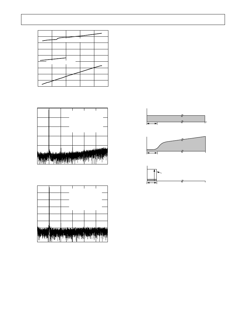
CIRCUIT DESCRIPTION
The AD7723 ADC employs a sigma-delta conversion technique
to convert the analog input into an equivalent digital word. The
modulator samples the input waveform and outputs an equiva-
lent digital word at the input clock frequency, f
CLKIN
.
Due to the high oversampling rate, which spreads the quantiza-
tion noise from 0 to f
CLKIN
/2, the noise energy contained in the
band of interest is reduced (Figure 24a). To further reduce the
quantization noise, a high order modulator is employed to shape
the noise spectrum, so that most of the noise energy is shifted
out of the band of interest (Figure 24b).
The digital filter that follows the modulator removes the large
out-of-band quantization noise, (Figure 24c) while also reduc-
ing the data rate from f
CLKIN
at the input of the filter to f
CLKIN
/32
or f
CLKIN
/16 at the output of the filter, depending on the state
on the MODE1/2 pins in parallel interface mode or the pin
SLDR in serial interface mode. The AD7723 output data rate is
a little over twice the signal bandwidth, which guarantees that
there is no loss of data in the signal band.
Digital filtering has certain advantages over analog filtering.
Firstly, since digital filtering occurs after the A/D conversion, it
can remove noise injected during the conversion process. Ana-
log filtering cannot remove noise injected during conversion.
Secondly, the digital filter combines low passband ripple with a
steep roll-off, while also maintaining a linear phase response.
NOISE SHAPING
QUANTIZATION NOISE
DIGITAL FILTER CUTOFF FREQUENCY
f
CLKIN
/2
f
CLKIN
/2
f
CLKIN
/2
BAND OF INTEREST
BAND OF INTEREST
BAND OF INTEREST
(a)
(b)
(c)
Figure 24. Sigma-Delta ADC
The AD7723 employs four or five Finite Impulse Response
(FIR) filters in series. Each individual filter’s output data rate is
half that of the filter’s input data rate. When data is fed to the
interface from the output of the fourth filter, the output data
rate is f
CLKIN
/16 and the resulting Over Sampling Ratio (OSR)
of the converter is 16. Data fed to the interface from the output
of the fifth filter results in an output data rate of f
CLKIN
/32 and a
corresponding OSR for the converter of 32. When an Output
Data Rate (ODR) of f
CLKIN
/32 is selected, the digital filter re-
sponse can be set to either low-pass or band-pass. The band-
pass response is useful when the input signal is band limited
since the resulting output data rate is half that required to con-
vert the band when the low pass operating mode is used. To
illustrate the operation of this mode, consider a band-limited
signal as shown in Figure 25a. This signal band can be correctly
converted by selecting the (low pass) ODR = f
CLKIN
/16 mode, as
shown in Figure 25b. Note that the output data rate is a little
over twice the maximum frequency in the frequency band. Alterna-
tively the band-pass mode can be selected as shown in Figure 25c.
The band-pass filter removes unwanted signals from dc to just
below f
CLKIN
/64. Rather than outputting data at f
CLKIN
/16, the
output of the band-pass filter is sampled at f
CLKIN
/32. This
相關PDF資料 |
PDF描述 |
|---|---|
| AD7723BS | 16-Bit, 1.2 MSPS CMOS, Sigma-Delta ADC |
| AD7724AST | Dual CMOS Modulators |
| AD7724 | Dual CMOS Modulators |
| AD7725 | 16-Bit 900 kSPS ADC with a Programmable Postprocessor |
| AD7725BS | 16-Bit 900 kSPS ADC with a Programmable Postprocessor |
相關代理商/技術參數(shù) |
參數(shù)描述 |
|---|---|
| AD7723BS | 制造商:Analog Devices 功能描述:ADC Single Delta-Sigma 19.2Msps 16-bit Parallel/Serial 44-Pin MQFP 制造商:Analog Devices 功能描述:Analog-Digital Converter IC Number of Bi |
| AD7723BS-REEL | 制造商:Analog Devices 功能描述:Single ADC Delta-Sigma 19.2Msps 16-bit Parallel/Serial 44-Pin MQFP T/R |
| AD7723BSZ | 功能描述:IC ADC 16BIT SIGMA-DELTA 44MQFP RoHS:是 類別:集成電路 (IC) >> 數(shù)據(jù)采集 - 模數(shù)轉(zhuǎn)換器 系列:- 其它有關文件:TSA1204 View All Specifications 標準包裝:1 系列:- 位數(shù):12 采樣率(每秒):20M 數(shù)據(jù)接口:并聯(lián) 轉(zhuǎn)換器數(shù)目:2 功率耗散(最大):155mW 電壓電源:模擬和數(shù)字 工作溫度:-40°C ~ 85°C 安裝類型:表面貼裝 封裝/外殼:48-TQFP 供應商設備封裝:48-TQFP(7x7) 包裝:Digi-Reel® 輸入數(shù)目和類型:4 個單端,單極;2 個差分,單極 產(chǎn)品目錄頁面:1156 (CN2011-ZH PDF) 其它名稱:497-5435-6 |
| AD7723BSZ1 | 制造商:AD 制造商全稱:Analog Devices 功能描述:16-Bit, 1.2 MSPS CMOS, Sigma-Delta ADC |
| AD7723BSZ-REEL | 功能描述:IC ADC 16BIT SIGMA-DELTA 44MQFP RoHS:是 類別:集成電路 (IC) >> 數(shù)據(jù)采集 - 模數(shù)轉(zhuǎn)換器 系列:- 標準包裝:1 系列:- 位數(shù):14 采樣率(每秒):83k 數(shù)據(jù)接口:串行,并聯(lián) 轉(zhuǎn)換器數(shù)目:1 功率耗散(最大):95mW 電壓電源:雙 ± 工作溫度:0°C ~ 70°C 安裝類型:通孔 封裝/外殼:28-DIP(0.600",15.24mm) 供應商設備封裝:28-PDIP 包裝:管件 輸入數(shù)目和類型:1 個單端,雙極 |
發(fā)布緊急采購,3分鐘左右您將得到回復。