- 您現(xiàn)在的位置:買賣IC網(wǎng) > PDF目錄373916 > AD7760BCP (ANALOG DEVICES INC) 2.5 MSPS, 20-Bit ADC PDF資料下載
參數(shù)資料
| 型號: | AD7760BCP |
| 廠商: | ANALOG DEVICES INC |
| 元件分類: | ADC |
| 英文描述: | 2.5 MSPS, 20-Bit ADC |
| 中文描述: | 1-CH 20-BIT DELTA-SIGMA ADC, PARALLEL ACCESS, QCC48 |
| 封裝: | LFCSP-48 |
| 文件頁數(shù): | 20/22頁 |
| 文件大小: | 868K |
| 代理商: | AD7760BCP |
AD7760
Preliminary Technical Data
AD7760 REGISTERS
The AD7760 has a number of user-programmable registers. The control registers are used to set the decimation rate, the filter
configuration, the clock divider etc. There are also digital gain, offset and over-range threshold registers. Writing to these registers
involves writing the register address first, then a 16-bit data word. Register Addresses, details of individual bits and default values are given
here.
Rev. PrN | Page 20 of 22
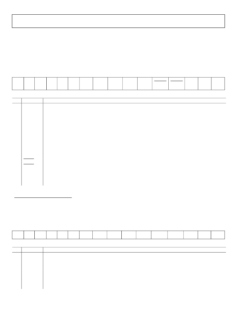
Table 12. Control Register 1 (Address 0x0001, Default Value 0x001A)
MSB
LSB
DL
Filt
RD
Ovr
RD
Gain
RD
Off
RD
Stat
CAL
SYNC
FLEN3
FLEN2
FLEN1
FLEN0
BYP F3
BYP F1
DEC2
DEC1
DEC0
Bit
15
Mnemonic
DL Filt
1
Comment
Download Filter. Before downloading a user defined filter, this bit must be set. The Filter Length bits must also be set at
this time. The write operations that follow will be interpreted as the user coefficients for the FIR filter until all the
coefficients and the checksum have been written.
Read Overrange. If this bit has been set, the next read operation will output the contents of the Overrange Threshold
Register instead of a conversion result.
Read Gain. If this bit has been set, the next read operation will output the contents of the digital Gain Register.
Read Offset. If this bit has been set, the next read operation will output the contents of the digital Offset Register.
Read Status. If this bit has been set, the next read operation will output the contents of the Status Register.
Calibration. Setting this bit will initiate an internal calibration routine. This routine will take 14mS with a 20MHz ICLK.
Synchronize. Setting this bit will initiate in internal synchronisation routine. Setting this bit simultaneously on multiple
devices will synchronize all filters.
Filter Length Bits. These bits must be set when the DL Filt bit is set and before a user defined filter is downloaded.
Bypass Filter 3. If this bit is a 0, Filter 3 (Programmable FIR) will be bypassed.
Bypass Filter 1. If this bit is a 0, Filter 1 will be bypassed. This should only occur when the user requires unfiltered
modulator data to be output.
Decimation Rate. These bits set the decimation rate of Filter 2. All zeros implies that the filter is bypassed. A value of 1
corresponds to 2x decimation, a value of 2 corresponds to 4x and so on up to the maximum value of 5, corresponding
to 32x decimation.
14
RD Ovr
1,2
13
12
11
10
9
RD Gain
1,2
RD Off
1,2
RD Stat
1,2
CAL
1
SYNC
1
8-5
4
3
FLEN3:0
BYP F3
BYP F1
2-0
DEC2:0
1
Bits 15-9 are all self clearing bits.
2
Only one of the bits 14-11 may be set in any write operation as they all determine the contents of the next read operation
Table 13. Control Register 2 (Address 0x0002, Default Value 0x009B)
MSB
LSB
0
0
0
0
0
0
0
0
0
0
CDIV1
CDIV0
PD
LPWR
1
D1PD
Bit
5-4
Mnemonic
CDIV1:0
Comment
Clock Divider Bits. These set the divide ratio of the MCLK signal to produce the internal ICLK. Setting CDIV[1:0] = 00
divides the MCLK by 2, setting CDIV[1:0] = 01 divides MCLK by 4. If CDIV[1:0] = 10 then the MCLK frequency is equal to
the ICLK. CDIV[1:0] = 11 is not allowed.
Power Down. Setting this bit powers down the AD7760 reducing the power consumption to TBD μW.
Low Power. If this bit is set, the AD7760 is operating in a low power mode. The power consumption is reduced for a 6dB
reduction in noise performance.
Write a ‘1’ to this bit.
Differential Amplifier Power Down. Setting this bit powers down the on-chip differential amplifier.
3
2
PD
LPWR
1
0
D1PD
相關(guān)PDF資料 |
PDF描述 |
|---|---|
| AD7760BSV | 2.5 MSPS, 20-Bit ADC |
| AD7769 | LC2MOS Analog I/O Port |
| AD7769AN | LC2MOS Analog I/O Port |
| AD7769AP | LC2MOS Analog I/O Port |
| AD7769JN | LC2MOS Analog I/O Port |
相關(guān)代理商/技術(shù)參數(shù) |
參數(shù)描述 |
|---|---|
| AD7760BCPZ | 制造商:Analog Devices 功能描述:2.5MSPS 18/20 BIT SIGMA DELTA ADC - Bulk |
| AD7760BST | 制造商:Analog Devices 功能描述:2.5MSPS 18/20 BIT SIGMA DELTA ADC - Bulk |
| AD7760BSV | 制造商:AD 制造商全稱:Analog Devices 功能描述:2.5 MSPS, 20-Bit ADC |
| AD7760BSVZ | 功能描述:IC ADC 24BIT 2.5MSPS 64TQFP RoHS:是 類別:集成電路 (IC) >> 數(shù)據(jù)采集 - 模數(shù)轉(zhuǎn)換器 系列:- 其它有關(guān)文件:TSA1204 View All Specifications 標(biāo)準(zhǔn)包裝:1 系列:- 位數(shù):12 采樣率(每秒):20M 數(shù)據(jù)接口:并聯(lián) 轉(zhuǎn)換器數(shù)目:2 功率耗散(最大):155mW 電壓電源:模擬和數(shù)字 工作溫度:-40°C ~ 85°C 安裝類型:表面貼裝 封裝/外殼:48-TQFP 供應(yīng)商設(shè)備封裝:48-TQFP(7x7) 包裝:Digi-Reel® 輸入數(shù)目和類型:4 個單端,單極;2 個差分,單極 產(chǎn)品目錄頁面:1156 (CN2011-ZH PDF) 其它名稱:497-5435-6 |
| AD7760BSVZ-REEL | 功能描述:IC ADC 24BIT 2.5MSPS 64TQFP RoHS:是 類別:集成電路 (IC) >> 數(shù)據(jù)采集 - 模數(shù)轉(zhuǎn)換器 系列:- 標(biāo)準(zhǔn)包裝:1 系列:- 位數(shù):14 采樣率(每秒):83k 數(shù)據(jù)接口:串行,并聯(lián) 轉(zhuǎn)換器數(shù)目:1 功率耗散(最大):95mW 電壓電源:雙 ± 工作溫度:0°C ~ 70°C 安裝類型:通孔 封裝/外殼:28-DIP(0.600",15.24mm) 供應(yīng)商設(shè)備封裝:28-PDIP 包裝:管件 輸入數(shù)目和類型:1 個單端,雙極 |
發(fā)布緊急采購,3分鐘左右您將得到回復(fù)。