- 您現(xiàn)在的位置:買賣IC網(wǎng) > PDF目錄373970 > AD9875 (Analog Devices, Inc.) Broadband Modem Mixed-Signal Front End PDF資料下載
參數(shù)資料
| 型號(hào): | AD9875 |
| 廠商: | Analog Devices, Inc. |
| 英文描述: | Broadband Modem Mixed-Signal Front End |
| 中文描述: | 寬帶調(diào)制解調(diào)器混合信號(hào)前端 |
| 文件頁(yè)數(shù): | 20/24頁(yè) |
| 文件大小: | 288K |
| 代理商: | AD9875 |
第1頁(yè)第2頁(yè)第3頁(yè)第4頁(yè)第5頁(yè)第6頁(yè)第7頁(yè)第8頁(yè)第9頁(yè)第10頁(yè)第11頁(yè)第12頁(yè)第13頁(yè)第14頁(yè)第15頁(yè)第16頁(yè)第17頁(yè)第18頁(yè)第19頁(yè)當(dāng)前第20頁(yè)第21頁(yè)第22頁(yè)第23頁(yè)第24頁(yè)
REV. 0
AD9875
–20–
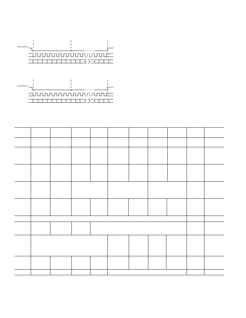
Figures 10a and 10b show how the serial port words are built
for each of these modes.
SENABLE
SCLK
SDATA
R/WI6
(N)
I5
(N)
I3
I4
I2
I1
I0
D7
N
D6
N
D2
0
D1
0
D0
0
INSTRUCTION CYCLE
DATA TRANSFER CYCLE
Figure 10a. Serial Register Interface Timing MSB-First
SENABLE
SCLK
SDATA
I0
I6
(N)
I5
(N)
I3
I4
I2
I1
R/W
D7
N
D6
N
D2
0
D1
0
D0
0
INSTRUCTION CYCLE
DATA TRANSFER CYCLE
Figure 10b. Serial Register Interface Timing LSB-First
Notes on Serial Port Operation
T he serial port is disabled and all registers are set to their default
values during a hardware reset. During a software reset, all
registers except register 0 are set to their default values. Register
0 will remain at the last value sent, with the exception that the
Software Reset
bit will be set to 0.
T he serial port is operated by an internal state machine and is
dependent on the number of SCLK cycles since the last time
SENABLE
went active. On every eighth rising edge of SCLK , a
byte is transferred over the SPI. During a multibyte write cycle,
this means the registers of the AD9875 are not simultaneously
updated, but occur sequentially. For this reason, it is recom-
mended that single byte transfers be used when changing the
SPI configuration or performing a software reset.
T able IV. Register Layout
Address
(hex)
Default
(hex)
0
×
00
Bit 7
Bit 6
Bit 5
Bit 4
Bit 3
Bit 2
Bit 1
Bit 0
Comments
0
SPI
LSB First
Software
Reset
Read/Write
1
Power-
Down
Regulator
Power-
Down
PLL-B
Power-
Down
PLL-A
Power-
Down
DAC
Power-
Down
Interpolator
Power-
Down
Rx
Reference
Power-
Down
ADC and
FPGA
Power-
Down
Rx LPF and
CPGA
0
×
00
Read/Write
PWR DN
Pin Low
2
Power-
Down
Regulator
Power-
Down
PLL-B
Power-
Down
PLL-A
Power-
Down
DAC
Power-
Down
Interpolator
Power-
Down
Rx
Reference
Power-
Down
ADC and
FPGA
Power-
Down
Rx LPF and
CPGA
0
×
9F
Read/Write
PWR DN
Pin High
3
T x Port
Negative
Edge
Sampling
ADC Clock
Source
PLL-B/2
PLL-B
(
×
M) Multiplier
< 5:4>
PLL-B
(
) Divider
< 3:3>
PLL-A
(
×
M) Multiplier
< 1:0>
0
×
02
Read/Write
4
T x Port
T uning
Update
Disable
Rx LPF
T uning
In Progress
(Read Only)
Rx Path
DC Offset
Correction Bypass
Rx Digital Fast ADC
HPF
Wideband
Rx LPF
Enable
1-Pole
Rx LPF
Rx LPF
Bypass
0
×
01
Read/Write
Sampling
5
Rx LPF Fc Adjust <4:0>
0
×
80
0
×
00
Read/Write
6
PGA
Gain Set
by Register
Rx Path Gain Adjust <4:0>
Read/Write
7
Interpolation Filter Select
<3:0>
Power-Down
Interpolator
at
T x QUIET
Pin Low
T x Port
LS Nibble
First
T x Port
Width
5-bits
T x Port
Multiplexer
Bypass
0
×
00
Read/Write
8
Invert
CLK B
Invert
CLK B
Invert
CLK B
Invert
CLK B
T hree-State
Rx Port
Rx Port
LS Nibble
First
Rx Port
Width
5-bits
Rx Port
Multiplexer
Bypass
0
×
00
Read/ Write
F
Die Revision Number <3:0>
Read Only
相關(guān)PDF資料 |
PDF描述 |
|---|---|
| AD9875-EB | Broadband Modem Mixed-Signal Front End |
| AD9875BST | Broadband Modem Mixed-Signal Front End |
| AD9876 | Broadband Modem Mixed-Signal Front End |
| AD9876-EB | Broadband Modem Mixed-Signal Front End |
| AD9876BST | Broadband Modem Mixed-Signal Front End |
相關(guān)代理商/技術(shù)參數(shù) |
參數(shù)描述 |
|---|---|
| AD9875BST | 制造商:Analog Devices 功能描述:Modem Chip Single 48-Pin LQFP 制造商:Rochester Electronics LLC 功能描述:10B BROADBAND MODEM MXFE CONVERTER - Tape and Reel |
| AD9875BSTRL | 制造商:Analog Devices 功能描述:Modem Chip Single 48-Pin LQFP T/R |
| AD9875BSTZ | 制造商:Analog Devices 功能描述:Modem Chip Single 48-Pin LQFP |
| AD9875-EB | 制造商:Analog Devices 功能描述: |
| AD9876 | 制造商:AD 制造商全稱:Analog Devices 功能描述:Broadband Modem Mixed-Signal Front End |
發(fā)布緊急采購(gòu),3分鐘左右您將得到回復(fù)。