- 您現在的位置:買賣IC網 > PDF目錄374037 > ADSP-BF531 (Analog Devices, Inc.) Blackfin Embedded Processor PDF資料下載
參數資料
| 型號: | ADSP-BF531 |
| 廠商: | Analog Devices, Inc. |
| 元件分類: | 數字信號處理 |
| 英文描述: | Blackfin Embedded Processor |
| 中文描述: | Blackfin嵌入式處理器 |
| 文件頁數: | 21/56頁 |
| 文件大小: | 671K |
| 代理商: | ADSP-BF531 |
第1頁第2頁第3頁第4頁第5頁第6頁第7頁第8頁第9頁第10頁第11頁第12頁第13頁第14頁第15頁第16頁第17頁第18頁第19頁第20頁當前第21頁第22頁第23頁第24頁第25頁第26頁第27頁第28頁第29頁第30頁第31頁第32頁第33頁第34頁第35頁第36頁第37頁第38頁第39頁第40頁第41頁第42頁第43頁第44頁第45頁第46頁第47頁第48頁第49頁第50頁第51頁第52頁第53頁第54頁第55頁第56頁
ADSP-BF531/ADSP-BF532/ADSP-BF533
Rev. 0
|
Page 21 of 56
|
March 2004
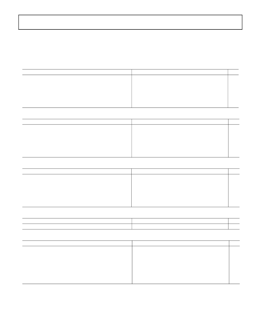
TIMING SPECIFICATIONS
Table 10
through
Table 14
describe the timing requirements for
the ADSP-BF531/2/3 processor clocks. Take care in selecting
MSEL, SSEL, and CSEL ratios so as not to exceed the maximum
core clock and system clock as described in
Absolute Maximum
Ratings on Page 20
, and the Voltage Controlled Oscillator
(VCO) operating frequencies described in
Table 13
.
Table 13
describes Phase-Locked Loop operating conditions.
Table 10. Core and System Clock Requirements—ADSP-BF533SKBC600
Parameter
t
CCLK
t
CCLK
t
CCLK
t
CCLK
t
CCLK
t
SCLK
Min
1.67
2.10
2.35
2.66
4.00
Maximum of 7.5 or t
CCLK
Max
Unit
ns
ns
ns
ns
ns
ns
Core Cycle Period (V
DDINT
=1.2 V–5%)
Core Cycle Period (V
DDINT
=1.1 V–5%)
Core Cycle Period (V
DDINT
=1.0 V–5%)
Core Cycle Period (V
DDINT
=0.9 V–5%)
Core Cycle Period (V
DDINT
=0.8 V)
System Clock Period
Table 11. Core and System Clock Requirements—ADSP-BF533SBBC500 and ADSP-BF533SBBZ500
Parameter
t
CCLK
t
CCLK
t
CCLK
t
CCLK
t
CCLK
t
SCLK
Min
2.0
2.25
2.50
3.00
4.00
Maximum of 7.5 or t
CCLK
Max
Unit
ns
ns
ns
ns
ns
ns
Core Cycle Period (V
DDINT
=1.2 V–5%)
Core Cycle Period (V
DDINT
=1.1 V–5%)
Core Cycle Period (V
DDINT
=1.0 V–5%)
Core Cycle Period (V
DDINT
=0.9 V–5%)
Core Cycle Period (V
DDINT
=0.8 V)
System Clock Period
Table 12. Core and System Clock Requirements—ADSP-BF532/531 All Package Types
Parameter
t
CCLK
t
CCLK
t
CCLK
t
CCLK
t
CCLK
t
SCLK
Min
2.5
2.75
3.00
3.25
4.0
Maximum of 7.5 or t
CCLK
Max
Unit
ns
ns
ns
ns
ns
ns
Core Cycle Period (V
DDINT
=1.2 V–5%)
Core Cycle Period (V
DDINT
=1.1 V–5%)
Core Cycle Period (V
DDINT
=1.0 V–5%)
Core Cycle Period (V
DDINT
=0.9 V–5%)
Core Cycle Period (V
DDINT
=0.8 V)
System Clock Period
Table 13. Phase-Locked Loop Operating Conditions
Parameter
f
VCO
Min
50
Max
Max CCLK
Unit
MHz
Voltage Controlled Oscillator (VCO) Frequency
Table 14. Maximum SCLK Conditions
Parameter
Condition
V
DDEXT
= 3.3 V
V
DDEXT
= 2.5 V
Unit
MBGA
f
SCLK
f
SCLK
LQFP
f
SCLK
f
SCLK
1
Set bit 7 (output delay) of PLL_CTL register.
V
DDINT
>=
1.14 V
V
DDINT
<
1.14 V
133
100
133
100
MHz
MHz
V
DDINT
>=
1.14 V
V
DDINT
<
1.14 V
133
83
133
1
83
1
MHz
MHz
相關PDF資料 |
PDF描述 |
|---|---|
| ADSP-BF531SBBC400 | Metal Connector Backshell |
| ADSP-BF531SBBZ400 | Blackfin Embedded Processor |
| ADSP-BF531SBST400 | Circular Connector Series:97 |
| ADSP-BF532 | Blackfin Embedded Processor |
| ADSP-BF532SBBC400 | Blackfin Embedded Processor |
相關代理商/技術參數 |
參數描述 |
|---|---|
| ADSP-BF531SBB400 | 功能描述:IC DSP CTLR 16BIT 400MHZ 169-BGA RoHS:是 類別:集成電路 (IC) >> 嵌入式 - DSP(數字式信號處理器) 系列:Blackfin® 標準包裝:2 系列:StarCore 類型:SC140 內核 接口:DSI,以太網,RS-232 時鐘速率:400MHz 非易失內存:外部 芯片上RAM:1.436MB 電壓 - 輸入/輸出:3.30V 電壓 - 核心:1.20V 工作溫度:-40°C ~ 105°C 安裝類型:表面貼裝 封裝/外殼:431-BFBGA,FCBGA 供應商設備封裝:431-FCPBGA(20x20) 包裝:托盤 |
| ADSPBF531SBBC400 | 制造商:Analog Devices 功能描述: |
| ADSP-BF531SBBC400 | 功能描述:IC DSP CTLR 16B 400MHZ 160MBGA RoHS:否 類別:集成電路 (IC) >> 嵌入式 - DSP(數字式信號處理器) 系列:Blackfin® 標準包裝:2 系列:StarCore 類型:SC140 內核 接口:DSI,以太網,RS-232 時鐘速率:400MHz 非易失內存:外部 芯片上RAM:1.436MB 電壓 - 輸入/輸出:3.30V 電壓 - 核心:1.20V 工作溫度:-40°C ~ 105°C 安裝類型:表面貼裝 封裝/外殼:431-BFBGA,FCBGA 供應商設備封裝:431-FCPBGA(20x20) 包裝:托盤 |
| ADSP-BF531SBBC-400X | 制造商:Analog Devices 功能描述: |
| ADSP-BF531SBBC-ENG | 制造商:Analog Devices 功能描述: |
發布緊急采購,3分鐘左右您將得到回復。