- 您現在的位置:買賣IC網 > PDF目錄371042 > MC68302CFC20 (MOTOROLA INC) Integrated Multiprotocol Processor User’s Manual PDF資料下載
參數資料
| 型號: | MC68302CFC20 |
| 廠商: | MOTOROLA INC |
| 元件分類: | 微控制器/微處理器 |
| 英文描述: | Integrated Multiprotocol Processor User’s Manual |
| 中文描述: | RISC PROCESSOR, PQFP132 |
| 封裝: | PLASTIC, QFP-132 |
| 文件頁數: | 140/480頁 |
| 文件大小: | 1815K |
| 代理商: | MC68302CFC20 |
第1頁第2頁第3頁第4頁第5頁第6頁第7頁第8頁第9頁第10頁第11頁第12頁第13頁第14頁第15頁第16頁第17頁第18頁第19頁第20頁第21頁第22頁第23頁第24頁第25頁第26頁第27頁第28頁第29頁第30頁第31頁第32頁第33頁第34頁第35頁第36頁第37頁第38頁第39頁第40頁第41頁第42頁第43頁第44頁第45頁第46頁第47頁第48頁第49頁第50頁第51頁第52頁第53頁第54頁第55頁第56頁第57頁第58頁第59頁第60頁第61頁第62頁第63頁第64頁第65頁第66頁第67頁第68頁第69頁第70頁第71頁第72頁第73頁第74頁第75頁第76頁第77頁第78頁第79頁第80頁第81頁第82頁第83頁第84頁第85頁第86頁第87頁第88頁第89頁第90頁第91頁第92頁第93頁第94頁第95頁第96頁第97頁第98頁第99頁第100頁第101頁第102頁第103頁第104頁第105頁第106頁第107頁第108頁第109頁第110頁第111頁第112頁第113頁第114頁第115頁第116頁第117頁第118頁第119頁第120頁第121頁第122頁第123頁第124頁第125頁第126頁第127頁第128頁第129頁第130頁第131頁第132頁第133頁第134頁第135頁第136頁第137頁第138頁第139頁當前第140頁第141頁第142頁第143頁第144頁第145頁第146頁第147頁第148頁第149頁第150頁第151頁第152頁第153頁第154頁第155頁第156頁第157頁第158頁第159頁第160頁第161頁第162頁第163頁第164頁第165頁第166頁第167頁第168頁第169頁第170頁第171頁第172頁第173頁第174頁第175頁第176頁第177頁第178頁第179頁第180頁第181頁第182頁第183頁第184頁第185頁第186頁第187頁第188頁第189頁第190頁第191頁第192頁第193頁第194頁第195頁第196頁第197頁第198頁第199頁第200頁第201頁第202頁第203頁第204頁第205頁第206頁第207頁第208頁第209頁第210頁第211頁第212頁第213頁第214頁第215頁第216頁第217頁第218頁第219頁第220頁第221頁第222頁第223頁第224頁第225頁第226頁第227頁第228頁第229頁第230頁第231頁第232頁第233頁第234頁第235頁第236頁第237頁第238頁第239頁第240頁第241頁第242頁第243頁第244頁第245頁第246頁第247頁第248頁第249頁第250頁第251頁第252頁第253頁第254頁第255頁第256頁第257頁第258頁第259頁第260頁第261頁第262頁第263頁第264頁第265頁第266頁第267頁第268頁第269頁第270頁第271頁第272頁第273頁第274頁第275頁第276頁第277頁第278頁第279頁第280頁第281頁第282頁第283頁第284頁第285頁第286頁第287頁第288頁第289頁第290頁第291頁第292頁第293頁第294頁第295頁第296頁第297頁第298頁第299頁第300頁第301頁第302頁第303頁第304頁第305頁第306頁第307頁第308頁第309頁第310頁第311頁第312頁第313頁第314頁第315頁第316頁第317頁第318頁第319頁第320頁第321頁第322頁第323頁第324頁第325頁第326頁第327頁第328頁第329頁第330頁第331頁第332頁第333頁第334頁第335頁第336頁第337頁第338頁第339頁第340頁第341頁第342頁第343頁第344頁第345頁第346頁第347頁第348頁第349頁第350頁第351頁第352頁第353頁第354頁第355頁第356頁第357頁第358頁第359頁第360頁第361頁第362頁第363頁第364頁第365頁第366頁第367頁第368頁第369頁第370頁第371頁第372頁第373頁第374頁第375頁第376頁第377頁第378頁第379頁第380頁第381頁第382頁第383頁第384頁第385頁第386頁第387頁第388頁第389頁第390頁第391頁第392頁第393頁第394頁第395頁第396頁第397頁第398頁第399頁第400頁第401頁第402頁第403頁第404頁第405頁第406頁第407頁第408頁第409頁第410頁第411頁第412頁第413頁第414頁第415頁第416頁第417頁第418頁第419頁第420頁第421頁第422頁第423頁第424頁第425頁第426頁第427頁第428頁第429頁第430頁第431頁第432頁第433頁第434頁第435頁第436頁第437頁第438頁第439頁第440頁第441頁第442頁第443頁第444頁第445頁第446頁第447頁第448頁第449頁第450頁第451頁第452頁第453頁第454頁第455頁第456頁第457頁第458頁第459頁第460頁第461頁第462頁第463頁第464頁第465頁第466頁第467頁第468頁第469頁第470頁第471頁第472頁第473頁第474頁第475頁第476頁第477頁第478頁第479頁第480頁
Communications Processor (CP)
4-20
MC68302 USER’S MANUAL
MOTOROLA
NMSI mode. The SIMODE register is a memory-mapped read-write register cleared by re-
set.
SETZ—Set L1TXD to zero (valid only for the GCI interface)
0 = Normal operation
1 = L1TXD output set to a logic zero (used in GCI activation, refer to 4.4.2 GCI Inter-
face)
SYNC/SCIT—SYNC Mode/SCIT Select Support
SYNC is valid only in PCM mode.
0 = One pulse wide prior to the 8-bit data
1 = N pulses wide and envelopes the N-bit data
The SCIT (Special Circuit Interface T) interface mode is valid only in GCI mode.
0 = SCIT support disabled
1 = SCIT D-channel collision enabled. Bit 4 of channel 2 C/I used by the IMP for receiv-
ing indication on the availability of the S interface D channel.
SDIAG1–SDIAG0—Serial Interface Diagnostic Mode (NMSI1 Pins Only)
00 = Normal operation
01 = Automatic echo
The channel automatically retransmits the received data on a bit-by-bit basis. The
receiver operates normally, but the transmitter can only retransmit received data.
In this mode, L1GR is ignored.
10 = Internal loopback
The transmitter output (L1TXD) is internally connected to the receiver input
(L1RXD). The receiver and the transmitter operate normally. Transmitted data ap-
pears on the L1TXD pin, and any external data received on L1RXD pin is ignored.
In this mode, L1RQ is asserted normally, and L1GR is ignored.
11 = Loopback control
In this mode, the transmitter output (TXD1/L1TXD) is internally connected to the
receiver input (RXD1/L1RXD). The TXD1/L1TXD, TXD2, TXD3, RTS1, RTS2,
and RTS3 pins will be high, but L1TXD will be three-stated in IDL and PCM
modes. This mode may be used to accomplish multiplex mode loopback testing
without affecting the multiplexed layer 1 interface. It also prevents an SCC's indi-
vidual loopback (configured in the SCM) from affecting the pins of its associated
NMSI interface.
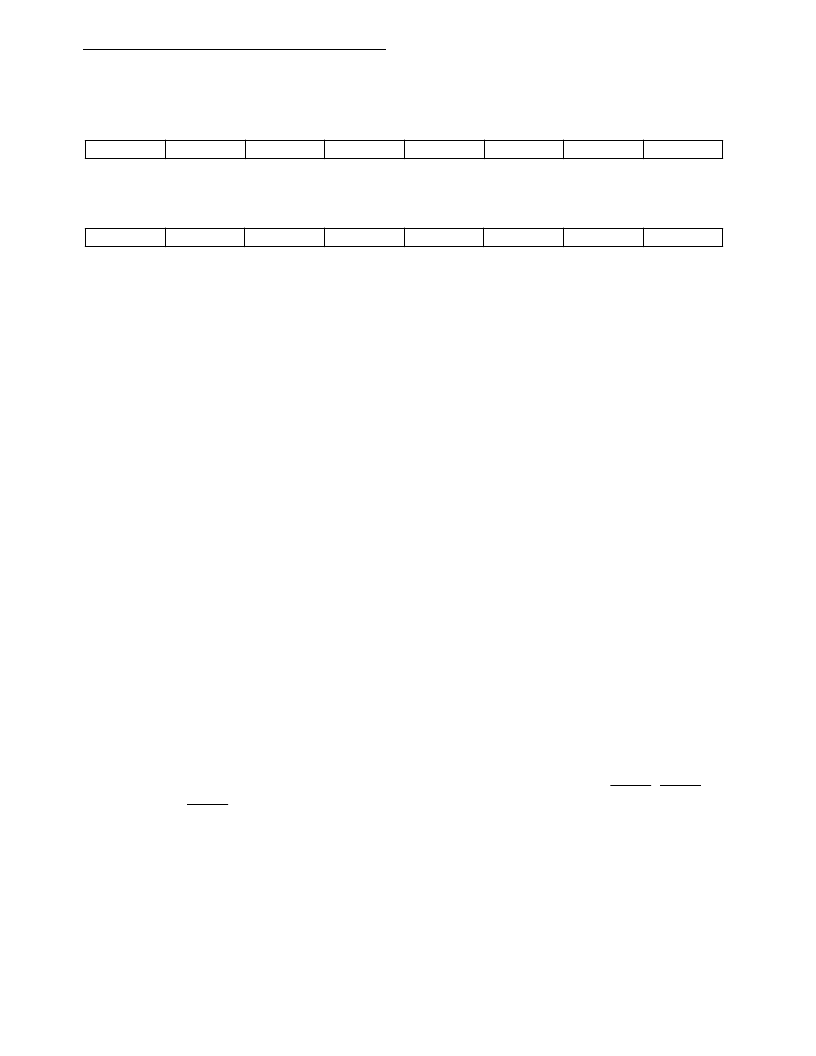
15
14
13
12
11
10
9
8
SETZ
SYNC/SCIT
SDIAG1
SDIAG0
SDC2
SDC1
B2RB
B2RA
7
6
5
4
3
2
1
0
B1RB
B1RA
DRB
DRA
MSC3
MSC2
MS1
MS0
相關PDF資料 |
PDF描述 |
|---|---|
| MC68302CRC16 | Integrated Multiprotocol Processor User’s Manual |
| MC68302CRC20 | Integrated Multiprotocol Processor User’s Manual |
| MC68302RC16 | Integrated Multiprotocol Processor User’s Manual |
| MC6802 | Microprocessor With Clock and Oprtional RAM |
| MC68B02P | Microprocessor With Clock and Oprtional RAM |
相關代理商/技術參數 |
參數描述 |
|---|---|
| MC68302CFC20C | 制造商:Motorola 功能描述:68302 |
| MC68302CFE16 | 制造商:未知廠家 制造商全稱:未知廠家 功能描述:Communications Controller |
| MC68302CFE20 | 制造商:未知廠家 制造商全稱:未知廠家 功能描述:Communications Controller |
| MC68302CPV16VC | 功能描述:IC MPU NETWORK 16MHZ 144-LQFP RoHS:否 類別:集成電路 (IC) >> 嵌入式 - 微處理器 系列:M683xx 標準包裝:2 系列:MPC8xx 處理器類型:32-位 MPC8xx PowerQUICC 特點:- 速度:133MHz 電壓:3.3V 安裝類型:表面貼裝 封裝/外殼:357-BBGA 供應商設備封裝:357-PBGA(25x25) 包裝:托盤 |
發布緊急采購,3分鐘左右您將得到回復。