- 您現(xiàn)在的位置:買賣IC網(wǎng) > PDF目錄371042 > MC68302CFC20 (MOTOROLA INC) Integrated Multiprotocol Processor User’s Manual PDF資料下載
參數(shù)資料
| 型號: | MC68302CFC20 |
| 廠商: | MOTOROLA INC |
| 元件分類: | 微控制器/微處理器 |
| 英文描述: | Integrated Multiprotocol Processor User’s Manual |
| 中文描述: | RISC PROCESSOR, PQFP132 |
| 封裝: | PLASTIC, QFP-132 |
| 文件頁數(shù): | 368/480頁 |
| 文件大小: | 1815K |
| 代理商: | MC68302CFC20 |
第1頁第2頁第3頁第4頁第5頁第6頁第7頁第8頁第9頁第10頁第11頁第12頁第13頁第14頁第15頁第16頁第17頁第18頁第19頁第20頁第21頁第22頁第23頁第24頁第25頁第26頁第27頁第28頁第29頁第30頁第31頁第32頁第33頁第34頁第35頁第36頁第37頁第38頁第39頁第40頁第41頁第42頁第43頁第44頁第45頁第46頁第47頁第48頁第49頁第50頁第51頁第52頁第53頁第54頁第55頁第56頁第57頁第58頁第59頁第60頁第61頁第62頁第63頁第64頁第65頁第66頁第67頁第68頁第69頁第70頁第71頁第72頁第73頁第74頁第75頁第76頁第77頁第78頁第79頁第80頁第81頁第82頁第83頁第84頁第85頁第86頁第87頁第88頁第89頁第90頁第91頁第92頁第93頁第94頁第95頁第96頁第97頁第98頁第99頁第100頁第101頁第102頁第103頁第104頁第105頁第106頁第107頁第108頁第109頁第110頁第111頁第112頁第113頁第114頁第115頁第116頁第117頁第118頁第119頁第120頁第121頁第122頁第123頁第124頁第125頁第126頁第127頁第128頁第129頁第130頁第131頁第132頁第133頁第134頁第135頁第136頁第137頁第138頁第139頁第140頁第141頁第142頁第143頁第144頁第145頁第146頁第147頁第148頁第149頁第150頁第151頁第152頁第153頁第154頁第155頁第156頁第157頁第158頁第159頁第160頁第161頁第162頁第163頁第164頁第165頁第166頁第167頁第168頁第169頁第170頁第171頁第172頁第173頁第174頁第175頁第176頁第177頁第178頁第179頁第180頁第181頁第182頁第183頁第184頁第185頁第186頁第187頁第188頁第189頁第190頁第191頁第192頁第193頁第194頁第195頁第196頁第197頁第198頁第199頁第200頁第201頁第202頁第203頁第204頁第205頁第206頁第207頁第208頁第209頁第210頁第211頁第212頁第213頁第214頁第215頁第216頁第217頁第218頁第219頁第220頁第221頁第222頁第223頁第224頁第225頁第226頁第227頁第228頁第229頁第230頁第231頁第232頁第233頁第234頁第235頁第236頁第237頁第238頁第239頁第240頁第241頁第242頁第243頁第244頁第245頁第246頁第247頁第248頁第249頁第250頁第251頁第252頁第253頁第254頁第255頁第256頁第257頁第258頁第259頁第260頁第261頁第262頁第263頁第264頁第265頁第266頁第267頁第268頁第269頁第270頁第271頁第272頁第273頁第274頁第275頁第276頁第277頁第278頁第279頁第280頁第281頁第282頁第283頁第284頁第285頁第286頁第287頁第288頁第289頁第290頁第291頁第292頁第293頁第294頁第295頁第296頁第297頁第298頁第299頁第300頁第301頁第302頁第303頁第304頁第305頁第306頁第307頁第308頁第309頁第310頁第311頁第312頁第313頁第314頁第315頁第316頁第317頁第318頁第319頁第320頁第321頁第322頁第323頁第324頁第325頁第326頁第327頁第328頁第329頁第330頁第331頁第332頁第333頁第334頁第335頁第336頁第337頁第338頁第339頁第340頁第341頁第342頁第343頁第344頁第345頁第346頁第347頁第348頁第349頁第350頁第351頁第352頁第353頁第354頁第355頁第356頁第357頁第358頁第359頁第360頁第361頁第362頁第363頁第364頁第365頁第366頁第367頁當前第368頁第369頁第370頁第371頁第372頁第373頁第374頁第375頁第376頁第377頁第378頁第379頁第380頁第381頁第382頁第383頁第384頁第385頁第386頁第387頁第388頁第389頁第390頁第391頁第392頁第393頁第394頁第395頁第396頁第397頁第398頁第399頁第400頁第401頁第402頁第403頁第404頁第405頁第406頁第407頁第408頁第409頁第410頁第411頁第412頁第413頁第414頁第415頁第416頁第417頁第418頁第419頁第420頁第421頁第422頁第423頁第424頁第425頁第426頁第427頁第428頁第429頁第430頁第431頁第432頁第433頁第434頁第435頁第436頁第437頁第438頁第439頁第440頁第441頁第442頁第443頁第444頁第445頁第446頁第447頁第448頁第449頁第450頁第451頁第452頁第453頁第454頁第455頁第456頁第457頁第458頁第459頁第460頁第461頁第462頁第463頁第464頁第465頁第466頁第467頁第468頁第469頁第470頁第471頁第472頁第473頁第474頁第475頁第476頁第477頁第478頁第479頁第480頁
MC68302 Applications
D-18
MC68302 USER’S MANUAL
MOTOROLA
initialization corresponds to the recommended order described in 4.5.7 SCC Initialization.
The second part is a set of loops waiting for data to arrive to be retransmitted out of the
SCC3. The third part is the SCC3 receive interrupt handler. Transmit interrupts are masked
in this example.
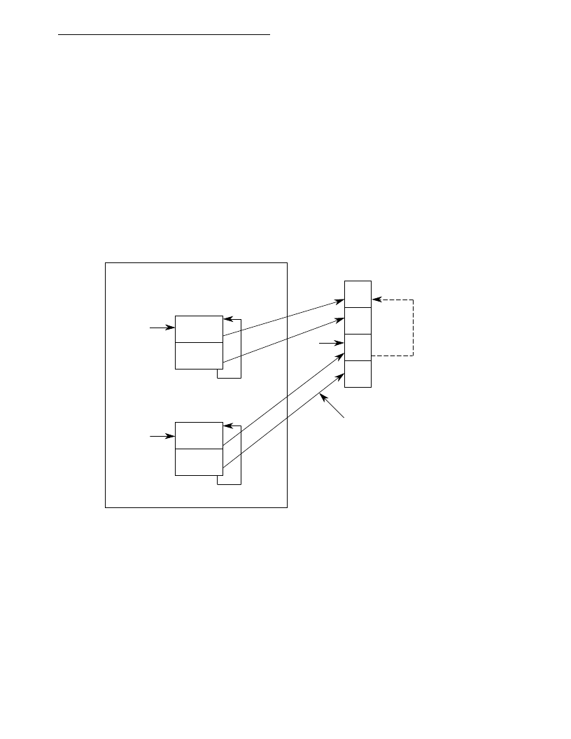
D.4.2 Organization of Buffers
In the MC68302, there is no such thing as an receive register (Rx) or transmit register (Tx).
Rather, a flexible structure called a buffer descriptor (BD) is used. In this example, two Rx
BDs and two Tx BDs are used. Each BD is set up to point to a one-byte location for data.
Thus, the receiver and transmitter are double-buffered. The number of Rx or Tx BDs can be
changed simply by changing the number of BDs initialized in the code (and two other lines
documented in the code). However, using at least two BDs has advantages as noted in the
following paragraphs.
The structure of the buffers is shown in Figure D-6.
Figure D-6. Transmit and Receive BD Tables and Buffers
To make the application more general, the data buffers were located in external RAM; how-
ever, internal RAM could have been used. Each BD points to just one byte in memory as
shown. Note that the data buffers do not need to be consecutive as shown.
From one to eight BDs may be used for both the transmit and receive operation. Use of eight
BDs for the transmit side of SCC3 requires that the SCP and SMCs not be used. As data
rates increase substantially beyond the 9600 baud of this example, the use of more BDs and
more data bytes per BD becomes justified. Why were two Rx BDs and two Tx BDs chosen
rather than just one each
BYTE
A2
SCC3 TRANSMIT BD TABLE
TX BD 0
TX BD 1
BYTE
BYTE
BYTE
$30000
$30001
$30002
$30003
A1
A0
RX BD 0
RX BD 1
DATA BUFFERS IN RAM
CPU MOVES
DATA FROM
RX TO TX
BUFFERS IN
THIS CODE.
MC68302
ON-CHIP DMA USES
THESE POINTERS TO KNOW
WHERE TO STORE DATA.
SCC3 RECEIVE BD TABLE
ONLY 2 OF 8 BDS ARE USED.
相關PDF資料 |
PDF描述 |
|---|---|
| MC68302CRC16 | Integrated Multiprotocol Processor User’s Manual |
| MC68302CRC20 | Integrated Multiprotocol Processor User’s Manual |
| MC68302RC16 | Integrated Multiprotocol Processor User’s Manual |
| MC6802 | Microprocessor With Clock and Oprtional RAM |
| MC68B02P | Microprocessor With Clock and Oprtional RAM |
相關代理商/技術參數(shù) |
參數(shù)描述 |
|---|---|
| MC68302CFC20C | 制造商:Motorola 功能描述:68302 |
| MC68302CFE16 | 制造商:未知廠家 制造商全稱:未知廠家 功能描述:Communications Controller |
| MC68302CFE20 | 制造商:未知廠家 制造商全稱:未知廠家 功能描述:Communications Controller |
| MC68302CPV16VC | 功能描述:IC MPU NETWORK 16MHZ 144-LQFP RoHS:否 類別:集成電路 (IC) >> 嵌入式 - 微處理器 系列:M683xx 標準包裝:2 系列:MPC8xx 處理器類型:32-位 MPC8xx PowerQUICC 特點:- 速度:133MHz 電壓:3.3V 安裝類型:表面貼裝 封裝/外殼:357-BBGA 供應商設備封裝:357-PBGA(25x25) 包裝:托盤 |
發(fā)布緊急采購,3分鐘左右您將得到回復。