- 您現在的位置:買賣IC網 > PDF目錄371089 > MCM64E918 (Motorola, Inc.) 8M Bit synchronous late write fast static RAM(8M位同步遲寫快速靜態RAM) PDF資料下載
參數資料
| 型號: | MCM64E918 |
| 廠商: | Motorola, Inc. |
| 英文描述: | 8M Bit synchronous late write fast static RAM(8M位同步遲寫快速靜態RAM) |
| 中文描述: | 晚8分位同步靜態隨機存儲器寫入速度(800萬位同步遲寫快速靜態內存) |
| 文件頁數: | 18/24頁 |
| 文件大小: | 503K |
| 代理商: | MCM64E918 |
MCM64E918
MCM64E836
18
MOTOROLA FAST SRAM
TEST ACCESS PORT PINS
TCK — TEST CLOCK (INPUT)
Clocks all TAP events. All inputs are captured on the rising
edge of TCK and all outputs propagate from the falling edge
of TCK.
TMS — TEST MODE SELECT (INPUT)
The TMS input is sampled on the rising edge of TCK. This
is the command input for the TAP controller state machine.
An undriven TMS input will produce the same result as a
logic 1 input level.
TDI — TEST DATA IN (INPUT)
The TDI input is sampled on the rising edge of TCK. This is
the input side of the serial registers placed between TDI and
TDO. The register placed between TDI and TDO is deter-
mined by the state of the TAP controller state machine and
the instruction that is currently loaded in the TAP instruction
register (refer to Figure 6). An undriven TDI pin will produce
the same result as a logic 1 input level.
TDO — TEST DATA OUT (OUTPUT)
Output that is active depending on the state of the TAP
state machine (refer to Figure 6). Output changes in
response to the falling edge of TCK. This is the output side of
the serial registers placed between TDI and TDO.
TRST — TAP RESET
This device does not have a TRST pin. TRST is optional in
IEEE 1149.1.
The test–logic reset state is entered while TMS
is held high for five rising edges of TCK. Power on reset cir-
cuitry is included internally. This type of reset does not affect
the operation of the system logic. The reset affects test logic
only.
TEST ACCESS PORT REGISTERS
OVERVIEW
The various TAP registers are selected (one at a time) via
the sequences of 1s and 0s input to the TMS pin as the TCK
is strobed. Each of the TAP registers are serial shift registers
that capture serial input data on the rising edge of TCK and
push serial data out on subsequent falling edge of TCK.
When a register is selected, it is “placed” between the TDI
and TDO pins.
INSTRUCTION REGISTER
The instruction register holds the instructions that are
executed by the TAP controller when it is moved into the run
test/idle or the various data register states. The instructions
are 3 bits long. The register can be loaded when it is placed
between the TDI and TDO pins. The instruction register is
automatically preloaded with the IDCODE instruction at
power up or whenever the controller is placed in test–logic–
reset state.
BYPASS REGISTER
The bypass register is a single bit register that can be
placed between TDI and TDO. It allows serial test data to be
passed through the RAMs TAP to another device in the scan
chain with as little delay as possible.
BOUNDARY SCAN REGISTER
The boundary scan register is identical in length to the
number of active input and I/O connections on the RAM (not
counting the TAP pins). This also includes a number of place
holder locations (always set to a logic 1) reserved for density
upgrade address pins. There are a total of 68 bits in the case
of the x36 device and 49 bits in the case of the x18 device.
The boundary scan register, under the control of the TAP
controller, is loaded with the contents of the RAMs I/O ring
when the controller is in capture–DR state and then is placed
between the TDI and TDO pins when the controller is moved
to shift–DR state. Several TAP instructions can be used to
activate the boundary scan register.
The Bump/Bit Scan Order tables describe which device
bump connects to each boundary scan register location. The
first column defines the bit’s position in the boundary scan
register. The shift register bit nearest TDO (i.e., first to be
shifted out) is defined as bit 1. The second column is the
name of the input or I/O at the bump and the third column is
the bump number.
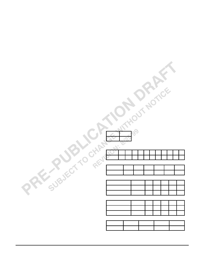
IDENTIFICATION (ID) REGISTER
The ID register is a 32–bit register that is loaded with a
device and vendor specific 32–bit code when the controller is
put in capture–DR state with the IDCODE command loaded
in the instruction register. The code is loaded from a 32–bit
on–chip ROM. It describes various attributes of the RAM as
indicated below. The register is then placed between the TDI
and TDO pins when the controller is moved into shift–DR
state. Bit 0 in the register is the LSB and the first to reach
TDO when shifting begins.
ID Register Presence Indicator
Bit No.
0
Value
1
Motorola JEDEC ID Code (Compressed Format, per
IEEE Standard 1149.1–1990
Bit No.
11
10
9
8
7
6
5
4
3
2
1
Value
0
0
0
0
0
0
0
1
1
1
0
Reserved For Future Use
Bit No.
17
16
15
14
13
12
Value
x
x
x
x
x
x
Device Width
Configuration
Bit No.
22
21
20
19
18
256K x 36
Value
0
0
1
0
0
512K x 18
Value
0
0
0
1
1
Device Depth
Configuration
Bit No.
27
26
25
24
23
256K x 36
Value
0
0
1
1
0
512K x 18
Value
0
0
1
1
1
Revision Number
Bit No.
31
30
29
28
Value
x
x
x
x
Figure 5. ID Register Bit Meanings
相關PDF資料 |
PDF描述 |
|---|---|
| MCM64PC32TSG66 | 256K/512K Pipelined BurstRAM Secondary Cache Module for Pentium |
| MCM64PC64TSG66 | 256K/512K Pipelined BurstRAM Secondary Cache Module for Pentium |
| MCM64PC32T | 256K/512K Pipelined BurstRAM Secondary Cache Module for Pentium |
| MCM6706RJ8 | 32K x 8 Bit Static Random Access Memory |
| MCM6706J6 | Circular Connector; Body Material:Aluminum; Series:PT06; Number of Contacts:41; Connector Shell Size:20; Connecting Termination:Crimp; Circular Shell Style:Straight Plug; Circular Contact Gender:Socket; Insert Arrangement:20-41 |
相關代理商/技術參數 |
參數描述 |
|---|---|
| MCM64PC32 | 制造商:MOTOROLA 制造商全稱:Motorola, Inc 功能描述:256K/512K Pipelined BurstRAM Secondary Cache Module for Pentium |
| MCM64PC32SG66 | 制造商:MOTOROLA 制造商全稱:Motorola, Inc 功能描述:256K/512K Pipelined BurstRAM Secondary Cache Module for Pentium |
| MCM64PC32T | 制造商:MOTOROLA 制造商全稱:Motorola, Inc 功能描述:256K/512K Pipelined BurstRAM Secondary Cache Module for Pentium |
| MCM64PC32TSG66 | 制造商:MOTOROLA 制造商全稱:Motorola, Inc 功能描述:256K/512K Pipelined BurstRAM Secondary Cache Module for Pentium |
| MCM64PC64SG66 | 制造商:MOTOROLA 制造商全稱:Motorola, Inc 功能描述:256K/512K Pipelined BurstRAM Secondary Cache Module for Pentium |
發布緊急采購,3分鐘左右您將得到回復。