- 您現在的位置:買賣IC網 > PDF目錄382345 > MPC9350 (Motorola, Inc.) LOW VOLTAGE PLL CLOCK DRIVER PDF資料下載
參數資料
| 型號: | MPC9350 |
| 廠商: | Motorola, Inc. |
| 英文描述: | LOW VOLTAGE PLL CLOCK DRIVER |
| 中文描述: | 低壓PLL時鐘驅動器 |
| 文件頁數: | 7/12頁 |
| 文件大小: | 282K |
| 代理商: | MPC9350 |
MPC9350
TIMING SOLUTIONS
MOTOROLA
Power Supply Filtering
The MPC9350 is a mixed analog/digital product and as such
it exhibits some sensitivities that would not necessarily be
seen on a fully digital product. Analog circuitry is naturally
susceptible to random noise, especially if this noise is seen on
the power supply pins. The MPC9350 provides separate
power supplies for the output buffers (VCCO) and the
phase-locked loop (VCCA) of the device.
The purpose of this design technique is to try and isolate the
high switching noise digital outputs from the relatively
sensitive internal analog phase-locked loop. In a controlled
environment such as an evaluation board this level of isolation
is sufficient. However, in a digital system environment where
it is more difficult to minimize noise on the power supplies a
second level ofisolation may be required. The simplest form of
isolation is a power supply filter on the VCCA pin for the
MPC9350. Figure 3. illustrates a typical power supply filter
scheme. The MPC9350 is most susceptible to noise with
spectral content in the 10kHz to 5MHz range. Therefore the
filter should be designed to target this range. The key
parameter that needs to be met in the final filter design is the
DC voltage drop that will be seen between the VCC supply and
the VCCA pin of the MPC9350. From the data sheet the IVCCA
current (the current sourced through the VCCA pin) is typically
10 mA (15 mA maximum), assuming that a minimum of 3.0V
must be maintained on the VCCA pin. Very little DC voltage
drop can be tolerated when a 3.3V VCC supply is used. The
resistor shown in Figure 3. “Power Supply Filter” must have
a resistance of 10-15 to meet the voltage drop criteria for
VCC=3.3V. For VCC=2.5V operation, RS must be selected to
maintain the minimum VCC specification of 2.375V for the PLL
supply pin for proper operation. The RC filter pictured will
provide a broadband filter with approximately 100:1
attenuation for noise whose spectral content is above 20 kHz.
As the noise frequency crosses the series resonant point of an
individual capacitor its overall impedance begins to look
inductive and thus increases with increasing frequency. The
parallel capacitor combination shown ensures that a low
impedance path to ground exists for frequencies well above
the bandwidth of the PLL. It is recommended that the user start
with an 8-10
resistor to avoid potential VCC drop problems
and only move to the higher value resistors when a higher level
of attenuation is shown to be needed.
Figure 3. Power Supply Filter
VCCA
VCC
MPC9350
0.01
μ
F
22
μ
F
0.01
μ
F
2.5V or 3.3V
RS=5–15
Although the MPC9350 has several design features to
minimize the susceptibility to power supply noise (isolated
power and grounds and fully differential PLL) there still may be
applications in which overall performance is being degraded
due to system power supply noise. The power supply filter
schemes discussed in this section should be adequate to
eliminate power supply noise related problems in most
designs.
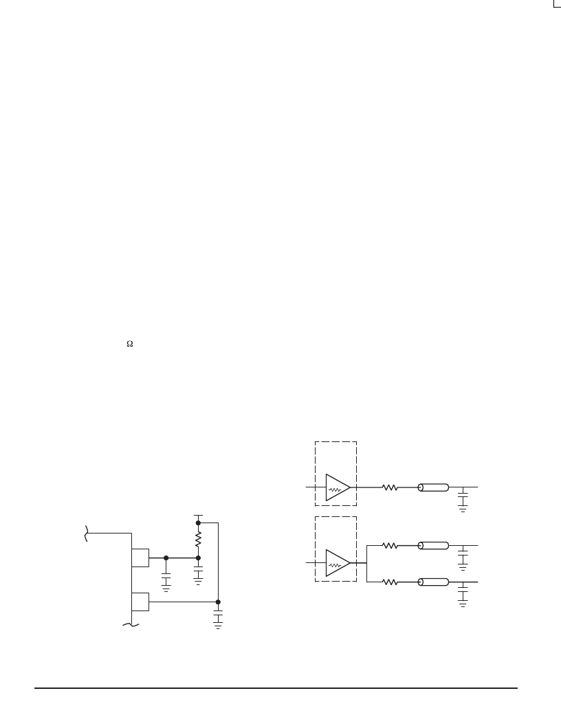
Driving Transmission Lines
The MPC9350 clock driver was designed to drive high
speed signals in a terminated transmission line environment.
To provide the optimum flexibility to the user the output drivers
were designed to exhibit the lowest impedance possible. With
an output impedance of less than 15
the drivers can drive
either parallel or series terminated transmission lines. For
more information on transmission lines the reader is referred
to Motorola application note AN1091. In most high
performance clock networks point-to-point distribution of
signals is the method of choice. In a point-to-point scheme
either series terminated or parallel terminated transmission
lines can be used. The parallel technique terminates the signal
at the end of the line with a 50
resistance to VCC
÷
2.
This technique draws a fairly high level of DC current and
thus only a single terminated line can be driven by each output
of the MPC9350 clock driver. For the series terminated case
however there is no DC current draw, thus the outputs can
drive multiple series terminated lines. Figure 4. “Single versus
Dual Transmission Lines” illustrates an output driving a single
series terminated line versus two series terminated lines in
parallel. When taken to its extreme the fanout of the MPC9350
clock driver is effectively doubled due to its capability to drive
multiple lines.
Figure 4. Single versus Dual Transmission Lines
14
IN
MPC9350
OUTPUT
BUFFER
RS = 36
ZO = 50
OutA
14
IN
MPC9350
OUTPUT
BUFFER
RS = 36
ZO = 50
OutB0
RS = 36
ZO = 50
OutB1
F
Freescale Semiconductor, Inc.
For More Information On This Product,
Go to: www.freescale.com
n
.
相關PDF資料 |
PDF描述 |
|---|---|
| MPC9350D | LOW VOLTAGE PLL CLOCK DRIVER |
| MPC9446 | 2.5V and 3.3V LVCMOS Clock Fanout Buffer |
| MPC9448 | 3.3V/2.5V LVCMOS 1:12 Clock Fanout Buffer |
| MPC9448D | 3.3V/2.5V LVCMOS 1:12 Clock Fanout Buffer |
| MPC9600 | LOW VOLTAGE 2.5 V AND 3.3 V CMOS PLL CLOCK DRIVER |
相關代理商/技術參數 |
參數描述 |
|---|---|
| MPC9350AC | 功能描述:時鐘驅動器及分配 2.5 3.3V 200MHz Clock Generator RoHS:否 制造商:Micrel 乘法/除法因子:1:4 輸出類型:Differential 最大輸出頻率:4.2 GHz 電源電壓-最大: 電源電壓-最小:5 V 最大工作溫度:+ 85 C 封裝 / 箱體:SOIC-8 封裝:Reel |
| MPC9350ACR2 | 功能描述:時鐘發生器及支持產品 FSL 1-9 LVCMOS PLL Clock Generator RoHS:否 制造商:Silicon Labs 類型:Clock Generators 最大輸入頻率:14.318 MHz 最大輸出頻率:166 MHz 輸出端數量:16 占空比 - 最大:55 % 工作電源電壓:3.3 V 工作電源電流:1 mA 最大工作溫度:+ 85 C 安裝風格:SMD/SMT 封裝 / 箱體:QFN-56 |
| MPC9350D | 制造商:MOTOROLA 制造商全稱:Motorola, Inc 功能描述:LOW VOLTAGE PLL CLOCK DRIVER |
| MPC9350FA | 功能描述:時鐘驅動器及分配 2.5 3.3V 200MHz Clock Generator RoHS:否 制造商:Micrel 乘法/除法因子:1:4 輸出類型:Differential 最大輸出頻率:4.2 GHz 電源電壓-最大: 電源電壓-最小:5 V 最大工作溫度:+ 85 C 封裝 / 箱體:SOIC-8 封裝:Reel |
| MPC9350FAR2 | 制造商:Integrated Device Technology Inc 功能描述:PLL Clock Driver Single 32-Pin LQFP T/R |
發布緊急采購,3分鐘左右您將得到回復。