- 您現在的位置:買賣IC網 > Datasheet目錄46 > SC418ULTRT (Semtech)IC REG DL BUCK/LINEAR 20MLPQ Datasheet資料下載
參數資料
| 型號: | SC418ULTRT |
| 廠商: | Semtech |
| 文件頁數: | 14/30頁 |
| 文件大小: | 691K |
| 描述: | IC REG DL BUCK/LINEAR 20MLPQ |
| 產品培訓模塊: | Power Supplies 101 |
| 標準包裝: | 1 |
| 系列: | EcoSpeed® |
| 拓撲: | 降壓(降壓)(1),線性(LDO)(1) |
| 功能: | 任何功能 |
| 輸出數: | 2 |
| 頻率 - 開關: | 1MHz |
| 電壓/電流 - 輸出 1: | 控制器 |
| 電壓/電流 - 輸出 2: | 0.75 V ~ 5.25 V,200mA |
| 帶 LED 驅動器: | 無 |
| 帶監控器: | 無 |
| 帶序列發生器: | 無 |
| 電源電壓: | 3 V ~ 28 V |
| 工作溫度: | -40°C ~ 85°C |
| 安裝類型: | 表面貼裝 |
| 封裝/外殼: | 20-MLPQ |
| 供應商設備封裝: | 20-MLPQ(3x3) |
| 包裝: | 標準包裝 |
| 其它名稱: | SC418ULTRTDKR |
第1頁第2頁第3頁第4頁第5頁第6頁第7頁第8頁第9頁第10頁第11頁第12頁第13頁當前第14頁第15頁第16頁第17頁第18頁第19頁第20頁第21頁第22頁第23頁第24頁第25頁第26頁第27頁第28頁第29頁第30頁
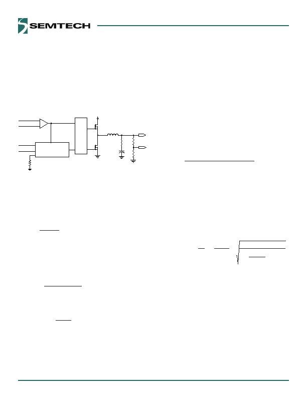
SC418
4
comparator and a capacitor. One comparator input is con-
nected to V
OUT
, the other input is connected to the
capacitor. When the on-time begins, the internal capaci-
tor charges from zero volts through a current which is
proportional to V
IN
. When the capacitor voltage reaches
V
OUT
, the on-time is completed and the high-side MOSFET
turns off.
Gate
Drives
FB Comparator
One-Shot
Timer
On-time = K x R
TON
x (V
OUT
/V
IN
)
OUT
IN
B
00mV
Q1
Q2
L
C
OUT
V
IN
ESR
+
V
OUT
V
LX
FB
DH
DL
TON
+
-
Figure 2 On-Time Generation
This method automatically produces an on-time that is
proportional to V
OUT
and inversely proportional to V
IN
.
Under steady-state conditions, the switching frequency
can be determined from the on-time by the following
equation.
IN
ON
OUT
SW
V
T
V
f
The SC48 uses an external resistor to set the on-time which
indirectly sets the frequency. The on-time can be pro-
grammed to provide an operating frequency from 200kHz
to MHz using a resistor between the TON pin and ground.
The resistor value is selected by the following equation.
OUT
IN
ON
TON
V
pF
25
V
)
ns
10
T
(
R
The maximum R
TON
value allowed is shown by the follow-
ing equation.
A
15
V
R
MIN
_
IN
MAX
_
TON
Immediately after the on-time, the DL output drives high
to energize the low-side MOSFET. DL has a minimum high
time of ~250ns, after which DL continues to stay high until
one of the following occurs:
VFB falls below the 500mV reference
"
The Zero Cross Detector trips if power-save is
active
TON Limitations and VDDA Supply Voltage
For VDDA below 4.5V, the TON accuracy may be limited
by V
IN
. The previous RTON equation is accurate if V
IN
satis-
fes the below relation over the entire V
IN
range:
V
IN
< (VDDA - 1.6V) x 10
If V
IN
exceeds ((VDDA - .6V) x 0) for all or part of the V
IN
range, the previous RTON equation is not accurate. In all
cases where VIN > ((VDDA - .6V) x 0), the RTON equation
must be modifi ed as follows.
OUT
ON
TON
V
25pF
10
1.6V)
(V5V
10ns)
(T
R
Note that when V
IN
is greater than ((VDDA - .6V) x 0), the
actual on-time is fixed and does not vary with V
IN
. When
operating in this condition, the switching frequency will
vary inversely with V
IN
rather than approximating fixed
frequency.
When a large capacitor is placed in parallel with R (CTOP)
VOUT is shown by the following equation.
2
TOP
1
2
1
2
2
TOP
1
RIPPLE
2
1
OUT
C
R
R
R
R
1
)
C
R
(
1
2
V
R
R
1
5
.
0
V
The switcher output voltage can be programmed higher
than 5V with careful design. In this case the VOUT pin
cannot connect directly to the switcher output due to its
the maximum voltage rating. An additional resistor
divider network is required to connect from the switcher
output to the VOUT pin. The voltage at the VOUT pin
should be at least 500mV lower than the VDDA supply, to
prevent the VLDO switch-over function. For example, the
voltage at the VOUT pin can be 4V if VDDA is set for 5V.
When the SC48 operates from an external power source
and the LDO is disabled by grounding the ENL pin, the
voltage at the VOUT pin can be as high as shown in
Recommended Operating Conditions. Note that RTON
must be adjusted higher by the same divider ratio to
"
Applications Information (continued)
相關PDF資料 |
PDF描述 |
|---|---|
| SC424MLTRT | IC REG DL BUCK/LINEAR 28MLPQ |
| SC4250LISTRT | IC HOT SWAP CTRLR 8-SOIC |
| SC427MLTRT | IC REG DL BUCK/LINEAR 32MLPQ |
| SE95D,112 | IC SENSOR TEMP 2.8-5.5V SOT96-1 |
| SE97BTP,547 | IC TEMP SENSOR DIMM 8HWSON |
相關代理商/技術參數 |
參數描述 |
|---|---|
| SC419 | 制造商:SEMTECH 制造商全稱:Semtech Corporation 功能描述:EcoSpeedTM DC-DC Converter with Integrated Boost Diode |
| SC419970CGCR2 | 制造商:Motorola Inc 功能描述: |
| SC419EVB | 制造商:SEMTECH 制造商全稱:Semtech Corporation 功能描述:EcoSpeedTM DC-DC Converter with Integrated Boost Diode |
| SC419ULTRT | 功能描述:IC REG CTRLR BUCK PWM 20-MLPQ RoHS:是 類別:集成電路 (IC) >> PMIC - 穩壓器 - DC DC 切換控制器 系列:EcoSpeed®, SmartDrive™ 特色產品:LM3753/54 Scalable 2-Phase Synchronous Buck Controllers 標準包裝:1 系列:PowerWise® PWM 型:電壓模式 輸出數:1 頻率 - 最大:1MHz 占空比:81% 電源電壓:4.5 V ~ 18 V 降壓:是 升壓:無 回掃:無 反相:無 倍增器:無 除法器:無 Cuk:無 隔離:無 工作溫度:-5°C ~ 125°C 封裝/外殼:32-WFQFN 裸露焊盤 包裝:Digi-Reel® 產品目錄頁面:1303 (CN2011-ZH PDF) 其它名稱:LM3754SQDKR |
| SC41E6 | 制造商:INFINEON 制造商全稱:Infineon Technologies AG 功能描述:SIEMENS ANNOUNCES A SUB-MICTON GENERATION OF CHANNELLESS GATE-ARRAYS BASED ON THE PROVEN MEGALOGIC PROCESS |
發布緊急采購,3分鐘左右您將得到回復。