- 您現(xiàn)在的位置:買賣IC網(wǎng) > Datasheet目錄46 > SC418ULTRT (Semtech)IC REG DL BUCK/LINEAR 20MLPQ Datasheet資料下載
參數(shù)資料
| 型號: | SC418ULTRT |
| 廠商: | Semtech |
| 文件頁數(shù): | 25/30頁 |
| 文件大小: | 691K |
| 描述: | IC REG DL BUCK/LINEAR 20MLPQ |
| 產(chǎn)品培訓(xùn)模塊: | Power Supplies 101 |
| 標準包裝: | 1 |
| 系列: | EcoSpeed® |
| 拓撲: | 降壓(降壓)(1),線性(LDO)(1) |
| 功能: | 任何功能 |
| 輸出數(shù): | 2 |
| 頻率 - 開關(guān): | 1MHz |
| 電壓/電流 - 輸出 1: | 控制器 |
| 電壓/電流 - 輸出 2: | 0.75 V ~ 5.25 V,200mA |
| 帶 LED 驅(qū)動器: | 無 |
| 帶監(jiān)控器: | 無 |
| 帶序列發(fā)生器: | 無 |
| 電源電壓: | 3 V ~ 28 V |
| 工作溫度: | -40°C ~ 85°C |
| 安裝類型: | 表面貼裝 |
| 封裝/外殼: | 20-MLPQ |
| 供應(yīng)商設(shè)備封裝: | 20-MLPQ(3x3) |
| 包裝: | 標準包裝 |
| 其它名稱: | SC418ULTRTDKR |
第1頁第2頁第3頁第4頁第5頁第6頁第7頁第8頁第9頁第10頁第11頁第12頁第13頁第14頁第15頁第16頁第17頁第18頁第19頁第20頁第21頁第22頁第23頁第24頁當(dāng)前第25頁第26頁第27頁第28頁第29頁第30頁
SC418
25
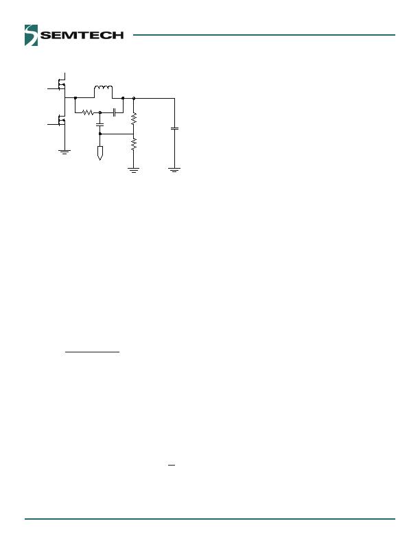
Applications Information (continued)
R1
R2
FB
pin
C
C
C
OUT
L
Low-
side
High-
side
C
L
R
L
Figure 15 Virtual ESR Ramp Current
This network creates a ramp voltage across C
L
, analogous
to the ramp voltage generated across the ESR of a stan-
dard capacitor. This ramp is then capacitively coupled into
the FB pin via capacitor C
C
.
Dropout Performance
The output voltage adjust range for continuous-conduc-
tion operation is limited by the fixed 250ns (typical)
minimum off-time of the one-shot. When working with
low input voltages, the duty-factor limit must be calcu-
lated using worst-case values for on and off times.
The duty-factor limitation is shown by the following
equation.
)
MAX
(
OFF
)
MIN
(
ON
)
MIN
(
ON
T
T
T
DUTY
The inductor resistance and MOSFET on-state voltage
drops must be included when performing worst-case
dropout duty-factor calculations.
System DC Accuracy (V
OUT
Controller)
Three factors affect V
OUT
accuracy: the trip point of the FB
error comparator, the ripple voltage variation with line
and load, and the external resistor tolerance. The error
comparator offset is trimmed so that under static condi-
tions it trips when the feedback pin is 500mV, + %.
The on-time pulse from the SC48 in the design example
is calculated to give a pseudo-fixed frequency of 250kHz.
Some frequency variation with line and load is expected.
This variation changes the output ripple voltage. Because
adaptive on-time converters regulate to the valley of the
output ripple, ?of the output ripple appears as a DC regu-
lation error. For example, if the output ripple is 50mV with
V
IN
= 6 volts, then the measured DC output will be 25mV
above the comparator trip point. If the ripple increases to
80mV with V
IN
= 25V, then the measured DC output will be
40mV above the comparator trip. The best way to mini-
mize this effect is to minimize the output ripple.
To compensate for valley regulation, it may be desirable to
use passive droop. Take the feedback directly from the
output side of the inductor and place a small amount of
trace resistance between the inductor and output capaci-
tor. This trace resistance should be optimized so that at
full load the output droops to near the lower regulation
limit. Passive droop minimizes the required output capaci-
tance because the voltage excursions due to load steps
are reduced as seen at the load.
The use of % feedback resistors contributes up to %
error. If tighter DC accuracy is required, 0.% resistors
should be used.
The output inductor value may change with current. This
will change the output ripple and therefore will have a
minor effect on the DC output voltage. The output ESR
also affects the output ripple and thus has a minor effect
on the DC output voltage.
Switching Frequency Variations
The switching frequency will vary depending on line and
load conditions. The line variations are a result of fixed
propagation delays in the on-time one-shot, as well as
unavoidable delays in the external MOSFET switching. As
V
IN
increases, these factors make the actual DH on-time
slightly longer than the ideal on-time. The net effect is
that frequency tends to falls slightly with increasing input
voltage.
The switching frequency also varies with load current as a
result of the power losses in the MOSFETs and the induc-
相關(guān)PDF資料 |
PDF描述 |
|---|---|
| SC424MLTRT | IC REG DL BUCK/LINEAR 28MLPQ |
| SC4250LISTRT | IC HOT SWAP CTRLR 8-SOIC |
| SC427MLTRT | IC REG DL BUCK/LINEAR 32MLPQ |
| SE95D,112 | IC SENSOR TEMP 2.8-5.5V SOT96-1 |
| SE97BTP,547 | IC TEMP SENSOR DIMM 8HWSON |
相關(guān)代理商/技術(shù)參數(shù) |
參數(shù)描述 |
|---|---|
| SC419 | 制造商:SEMTECH 制造商全稱:Semtech Corporation 功能描述:EcoSpeedTM DC-DC Converter with Integrated Boost Diode |
| SC419970CGCR2 | 制造商:Motorola Inc 功能描述: |
| SC419EVB | 制造商:SEMTECH 制造商全稱:Semtech Corporation 功能描述:EcoSpeedTM DC-DC Converter with Integrated Boost Diode |
| SC419ULTRT | 功能描述:IC REG CTRLR BUCK PWM 20-MLPQ RoHS:是 類別:集成電路 (IC) >> PMIC - 穩(wěn)壓器 - DC DC 切換控制器 系列:EcoSpeed®, SmartDrive™ 特色產(chǎn)品:LM3753/54 Scalable 2-Phase Synchronous Buck Controllers 標準包裝:1 系列:PowerWise® PWM 型:電壓模式 輸出數(shù):1 頻率 - 最大:1MHz 占空比:81% 電源電壓:4.5 V ~ 18 V 降壓:是 升壓:無 回掃:無 反相:無 倍增器:無 除法器:無 Cuk:無 隔離:無 工作溫度:-5°C ~ 125°C 封裝/外殼:32-WFQFN 裸露焊盤 包裝:Digi-Reel® 產(chǎn)品目錄頁面:1303 (CN2011-ZH PDF) 其它名稱:LM3754SQDKR |
| SC41E6 | 制造商:INFINEON 制造商全稱:Infineon Technologies AG 功能描述:SIEMENS ANNOUNCES A SUB-MICTON GENERATION OF CHANNELLESS GATE-ARRAYS BASED ON THE PROVEN MEGALOGIC PROCESS |
發(fā)布緊急采購,3分鐘左右您將得到回復(fù)。