- 您現在的位置:買賣IC網 > Datasheet目錄46 > SC418ULTRT (Semtech)IC REG DL BUCK/LINEAR 20MLPQ Datasheet資料下載
參數資料
| 型號: | SC418ULTRT |
| 廠商: | Semtech |
| 文件頁數: | 19/30頁 |
| 文件大小: | 691K |
| 描述: | IC REG DL BUCK/LINEAR 20MLPQ |
| 產品培訓模塊: | Power Supplies 101 |
| 標準包裝: | 1 |
| 系列: | EcoSpeed® |
| 拓撲: | 降壓(降壓)(1),線性(LDO)(1) |
| 功能: | 任何功能 |
| 輸出數: | 2 |
| 頻率 - 開關: | 1MHz |
| 電壓/電流 - 輸出 1: | 控制器 |
| 電壓/電流 - 輸出 2: | 0.75 V ~ 5.25 V,200mA |
| 帶 LED 驅動器: | 無 |
| 帶監控器: | 無 |
| 帶序列發生器: | 無 |
| 電源電壓: | 3 V ~ 28 V |
| 工作溫度: | -40°C ~ 85°C |
| 安裝類型: | 表面貼裝 |
| 封裝/外殼: | 20-MLPQ |
| 供應商設備封裝: | 20-MLPQ(3x3) |
| 包裝: | 標準包裝 |
| 其它名稱: | SC418ULTRTDKR |
第1頁第2頁第3頁第4頁第5頁第6頁第7頁第8頁第9頁第10頁第11頁第12頁第13頁第14頁第15頁第16頁第17頁第18頁當前第19頁第20頁第21頁第22頁第23頁第24頁第25頁第26頁第27頁第28頁第29頁第30頁
SC418
9
cycle. The switcher will shut off if VDDA falls below 2.7V.
VDDP does not have ULVO protection.
Note that the VDDA UVLO will not stop MOSFET switching
until the VDDA voltage falls to 2.7V. During this time the
gate driver voltages will track the VDDA supply. Not all
MOSFETs will operate or switch effectively at drive levels
of 2.7V. For this reason, it is not recommended to rely on
VDDA UVLO to shutdown the switcher unless the MOSFETs
are capable of operating with 2.7V drive.
LDO Regulator
The LDO output is programmable from 0.75V to 5.25V
using external resistors. The feedback pin (FBL) for the
LDO is regulated to 750mV. The LDO enable pin (ENL)
provides independent control. The LDO voltage can be
used to provide the bias voltage for the switching regula-
tor. When a separate source is used as the bias supply, the
LDO can be programmed to provide a different voltage.
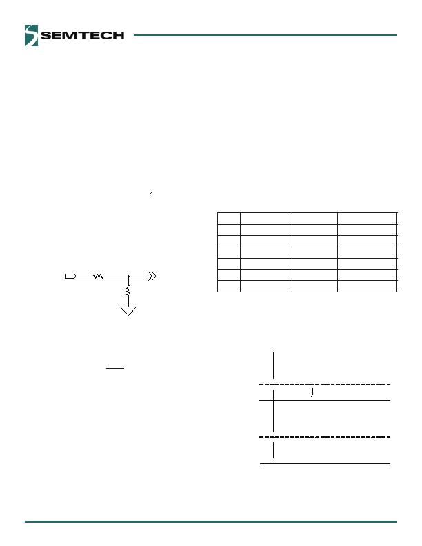
The external resistor connections are shown in Figure 0.
VLDO
To FBL pin
R
LDO2
R
LDO1
Figure 10 VLDO Resistor Divider
The LDO output voltage is set by the following equation.
2
LDO
1
LDO
R
R
1
mV
750
VLDO
A minimum capacitance of 糉 referenced to AGND is
normally required at the output of the LDO for stability. If
the LDO is providing bias power to the device, then a
minimum 0.糉 capacitor referenced to AGND is required,
along with a minimum 糉 capacitor referenced to PGND
to filter the gate drive pulses. Refer to the PCB Layout
Guidelines section.
ENL Pin and VIN UVLO
The ENL pin also acts as the V
IN
under-voltage lockout for
the switcher. The V
IN
UVLO voltage is programmable via a
resistor divider at the VIN, ENL and AGND pins. The V
IN
UVLO function has a typical threshold of 2.6V on the V
IN
rising edge. The falling edge threshold is 2.4V.
Timing is important when driving ENL with logic and not
implementing V
IN
UVLO. The ENL pin must transition from
high to low within 2 switching cycles to avoid the PWM
output turning off. If ENL goes below the V
IN
UVLO thresh-
old and stays above V, then the switcher will turn off but
the LDO will remain on.
Note that it is possible to operate the switcher with the
LDO disabled, but the ENL pin must be below the logic
low threshold (0.4V maximum), otherwise the V
IN
UVLO
function will disable the switcher.
The table below summarizes the function of the ENL and
EN pins, with respect to the rising edge of ENL.
EN
ENL LDO status Switcher status
low low, < 0.4V off
off
high low, < 0.4V off
on
low high, < 2.6V on
off
high high, < 2.6V on
off
low high, > 2.6V on
off
high high, > 2.6V on
on
Figure shows the ENL voltage thresholds and their
effect on LDO and Switcher operation.
AGND
ENL low
threshold
(min 0.4V)
2.6V
2.4V
LDO on
LDO on
LDO off
VIN UVLO hysteresis
ENL voltage
Switcher on if EN = high
Switcher on if EN = high
Switcher off by VIN UVLO
Figure 11 ENL Thresholds
Applications Information (continued)
相關PDF資料 |
PDF描述 |
|---|---|
| SC424MLTRT | IC REG DL BUCK/LINEAR 28MLPQ |
| SC4250LISTRT | IC HOT SWAP CTRLR 8-SOIC |
| SC427MLTRT | IC REG DL BUCK/LINEAR 32MLPQ |
| SE95D,112 | IC SENSOR TEMP 2.8-5.5V SOT96-1 |
| SE97BTP,547 | IC TEMP SENSOR DIMM 8HWSON |
相關代理商/技術參數 |
參數描述 |
|---|---|
| SC419 | 制造商:SEMTECH 制造商全稱:Semtech Corporation 功能描述:EcoSpeedTM DC-DC Converter with Integrated Boost Diode |
| SC419970CGCR2 | 制造商:Motorola Inc 功能描述: |
| SC419EVB | 制造商:SEMTECH 制造商全稱:Semtech Corporation 功能描述:EcoSpeedTM DC-DC Converter with Integrated Boost Diode |
| SC419ULTRT | 功能描述:IC REG CTRLR BUCK PWM 20-MLPQ RoHS:是 類別:集成電路 (IC) >> PMIC - 穩壓器 - DC DC 切換控制器 系列:EcoSpeed®, SmartDrive™ 特色產品:LM3753/54 Scalable 2-Phase Synchronous Buck Controllers 標準包裝:1 系列:PowerWise® PWM 型:電壓模式 輸出數:1 頻率 - 最大:1MHz 占空比:81% 電源電壓:4.5 V ~ 18 V 降壓:是 升壓:無 回掃:無 反相:無 倍增器:無 除法器:無 Cuk:無 隔離:無 工作溫度:-5°C ~ 125°C 封裝/外殼:32-WFQFN 裸露焊盤 包裝:Digi-Reel® 產品目錄頁面:1303 (CN2011-ZH PDF) 其它名稱:LM3754SQDKR |
| SC41E6 | 制造商:INFINEON 制造商全稱:Infineon Technologies AG 功能描述:SIEMENS ANNOUNCES A SUB-MICTON GENERATION OF CHANNELLESS GATE-ARRAYS BASED ON THE PROVEN MEGALOGIC PROCESS |
發布緊急采購,3分鐘左右您將得到回復。