- 您現在的位置:買賣IC網 > PDF目錄98215 > TFP9431CPAP (TEXAS INSTRUMENTS INC) SPECIALTY CONSUMER CIRCUIT, PQFP64 PDF資料下載
參數資料
| 型號: | TFP9431CPAP |
| 廠商: | TEXAS INSTRUMENTS INC |
| 元件分類: | 消費家電 |
| 英文描述: | SPECIALTY CONSUMER CIRCUIT, PQFP64 |
| 封裝: | 10 X 10 MM, 1.40 MM HEIGHT, 0.50 MM PITCH, POWER, THERMALLY ENHANCED, PLASTIC, TQFP-64 |
| 文件頁數: | 13/18頁 |
| 文件大?。?/td> | 241K |
| 代理商: | TFP9431CPAP |
TFP9431
PanelBus
DVI RECEIVER WITH TRIPLE DAC
SLDS122A – MARCH 2000 – REVISED JUNE 2000
4
POST OFFICE BOX 655303
DALLAS, TEXAS 75265
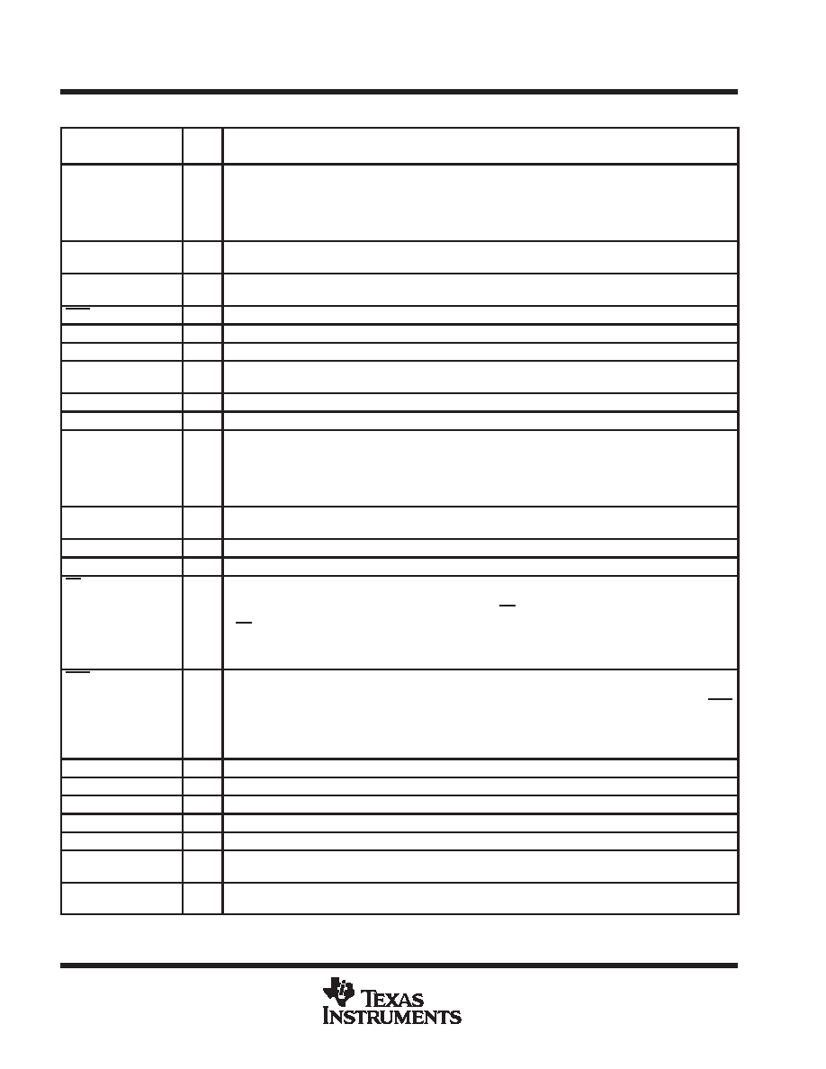
Terminal Functions (continued)
TERMINAL
I/O
DESCRIPTION
NAME
NO.
I/O
DESCRIPTION
DFO
7
DI
Output clock data format – Controls the output clock (ODCK) format for either TFT or DSTN panel support. For
TFT support ODCK clock runs continuously. For DSTN support ODCK only clocks when DE is high, otherwise
ODCK is held low when DE is low.
High : DSTN support/ODCK held low when DE = low
Low: TFT support/ODCK runs continuously.
EXT_RES
2
AI
Internal impedance matching – The TFP9431 is internally optimized for impedance matching at 50
.. An
external resistor tied to this pin an AVCC will have no effect on device performance.
FSADJ
21
A
Full scale adjust control – A 2 k
resistor should be connected between this pin and DACGND to control the
full scale output current on the analog outputs.
GND
11,17
GND
Digital ground – Ground reference and current return for digital core
GRNDAC
25
A
Analog green output
HS
30
DO
Horizontal sync output
NC
10,13,
38–40
DI
Reserved
NC
18,26
DI
Reserved
NC
41–48
DO
Reserved
OCK_INV
6
DI
ODCK Polarity – Selects ODCK edge on which pixel data and control signals (HSYNC, VSYNC, DE, CTL1-3 )
are latched
Normal Mode:
High : Latches output data on rising ODCK edge
Low : Latches output data on falling ODCK edge
ODCK
35
DO
Output data clock - Pixel clock. All pixel outputs GRNDAC,REDDAC, BLUDAC, and Q[7:0] along with DE,
HSYNC, VSYNC and CTL[3:1] are synchronized to this clock.
OGND
36
GND
Output driver ground – Ground reference and current return for digital output drivers
OVCC
34
VCC
Output driver VCC – Power supply for output drivers. Nominally 3.3 V
PD
8
DI
Power down – An active low signal that controls the TFP9431 power-down state. During power down all output
buffers are switched to a high impedance state and brought low through a weak pulldown. All analog circuits
are powered down and all inputs are disabled, except for PD.
If PD is left unconnected an internal pullup will default the TFP9431 to normal operation.
High : Normal operation
Low: Power down
PDO
15
DI
Output drive power down – An active low signal that controls the power-down state of the output drivers.
During output drive power down, the output drivers (except SCDT and CTL1) are driven to a high impedance
state and the DACs are switched off.. A weak pulldown will slowly pull these outputs to a low level. When PDO
is left unconnected, an internal pullup defaults the TFP9431 to normal operation.
High : Normal operation/output drivers on
Low: Output drive power down.
PGND
4
GND
PLL ground – Ground reference and current return for internal PLL
PVCC
3
VCC
PLL VCC – Power supply for internal PLL
REDDAC
23
A
Analog red output
RSVD
99
DI
Reserved. Must be tied high for normal operation.
RxC+
62
AI
Clock positive receiver input – Positive side of reference clock. TMDS low voltage signal differential input pair
RxC–
63
AI
Clock negative receiver input – Negative side of reference clock. TMDS low voltage signal differential input
pair.
Rx0+
59
AI
Channel-0 positive receiver input – Positive side of channel-0. TMDS low voltage signal differential input pair.
Channel-0 receives blue pixel data in active display and HSYNC, VSYNC control signals in blank.
相關PDF資料 |
PDF描述 |
|---|---|
| TG355ENK-7916 | 8.15 MHz, LOW PASS FILTER |
| TH355BDI-4957 | 4.43 MHz, BAND PASS FILTER |
| TH355LDK-7915 | 8.15 MHz, LOW PASS FILTER |
| TH355LNK-4550 | 10 MHz, LOW PASS FILTER |
| TH355LNK-4867 | 5 MHz, LOW PASS FILTER |
相關代理商/技術參數 |
參數描述 |
|---|---|
| TFP-AA-10T-13 | 制造商:DIALIGHT 制造商全稱:Dialight Corporation 功能描述:Tactical Composite Front Park Turn Light |
| TFPAA13B13 | 制造商:Dialight 功能描述: |
| TFPAA13D13 | 制造商:Dialight 功能描述: |
| TFPAA13T13 | 制造商:Dialight 功能描述: |
| TFP-AA-13T-13 | 制造商:DIALIGHT 制造商全稱:Dialight Corporation 功能描述:Tactical Composite Front Park Turn Light |
發布緊急采購,3分鐘左右您將得到回復。