- 您現在的位置:買賣IC網 > PDF目錄98215 > TFP9431CPAP (TEXAS INSTRUMENTS INC) SPECIALTY CONSUMER CIRCUIT, PQFP64 PDF資料下載
參數資料
| 型號: | TFP9431CPAP |
| 廠商: | TEXAS INSTRUMENTS INC |
| 元件分類: | 消費家電 |
| 英文描述: | SPECIALTY CONSUMER CIRCUIT, PQFP64 |
| 封裝: | 10 X 10 MM, 1.40 MM HEIGHT, 0.50 MM PITCH, POWER, THERMALLY ENHANCED, PLASTIC, TQFP-64 |
| 文件頁數: | 14/18頁 |
| 文件大小: | 241K |
| 代理商: | TFP9431CPAP |
TFP9431
PanelBus
DVI RECEIVER WITH TRIPLE DAC
SLDS122A – MARCH 2000 – REVISED JUNE 2000
5
POST OFFICE BOX 655303
DALLAS, TEXAS 75265
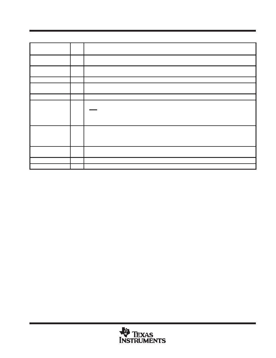
Terminal Functions (continued)
TERMINAL
I/O
DESCRIPTION
NAME
NO.
I/O
DESCRIPTION
Rx0–
60
AI
Channel-0 negative receiver input – Negative side of channel-0. TMDS low voltage signal differential input
pair.
Rx1+
54
AI
Channel-1 positive receiver input – Positive side of channel-1 TMDS low voltage signal differential input pair.
Channel-1 receives green pixel data in active display and CTL1 control signals in blank.
Rx1–
55
AI
Channel-1 negative receiver input – Negative side of channel-1 TMDS low voltage signal differential input pair
Rx2+
49
AI
Channel-2 positive receiver input – Positive side of channel-2 TMDS low voltage signal differential input pair.
Channel-2 receives red pixel data in active display and CTL2, CTL3 control signals in blank.
Rx2-
50
AI
Channel-2 negative receiver input – Negative side of channel-2 TMDS low voltage signal differential input pair.
SCDT
14
DO
Sync detect – Output to signal when the link is active or inactive. The link is considered to be active when DE is
actively switching. The TFP9431 monitors the state DE to determine link activity. SCDT can be tied externally
to PDO to power down the out put drivers when the link is inactive.
High: Active link
Low: Inactive link
ST
9
DI
Output drive strength select – Selects output drive strength for high or low current drive for digital outputs. (See
dc specifications for IOH and IOL vs ST state.)
High : High drive strength
Low : Low drive strength
TESTB
5
I
Test mode enable – This pin must be tied low for normal mode of operation. Connecting this pin to high puts
TFP9431 in test mode.
VCC
12, 16
VCC
Digital VCC – Power supply for digital core. Nominally 3.3 V
VS
29
DO
Vertical sync output
相關PDF資料 |
PDF描述 |
|---|---|
| TG355ENK-7916 | 8.15 MHz, LOW PASS FILTER |
| TH355BDI-4957 | 4.43 MHz, BAND PASS FILTER |
| TH355LDK-7915 | 8.15 MHz, LOW PASS FILTER |
| TH355LNK-4550 | 10 MHz, LOW PASS FILTER |
| TH355LNK-4867 | 5 MHz, LOW PASS FILTER |
相關代理商/技術參數 |
參數描述 |
|---|---|
| TFP-AA-10T-13 | 制造商:DIALIGHT 制造商全稱:Dialight Corporation 功能描述:Tactical Composite Front Park Turn Light |
| TFPAA13B13 | 制造商:Dialight 功能描述: |
| TFPAA13D13 | 制造商:Dialight 功能描述: |
| TFPAA13T13 | 制造商:Dialight 功能描述: |
| TFP-AA-13T-13 | 制造商:DIALIGHT 制造商全稱:Dialight Corporation 功能描述:Tactical Composite Front Park Turn Light |
發布緊急采購,3分鐘左右您將得到回復。