- 您現在的位置:買賣IC網 > PDF目錄98252 > TLV320ADC3001IYZHT (TEXAS INSTRUMENTS INC) 2-CH 16-BIT PROPRIETARY METHOD ADC, SERIAL ACCESS, PBGA16 PDF資料下載
參數資料
| 型號: | TLV320ADC3001IYZHT |
| 廠商: | TEXAS INSTRUMENTS INC |
| 元件分類: | ADC |
| 英文描述: | 2-CH 16-BIT PROPRIETARY METHOD ADC, SERIAL ACCESS, PBGA16 |
| 封裝: | GREEN, DSBGA-16 |
| 文件頁數: | 25/81頁 |
| 文件大小: | 836K |
| 代理商: | TLV320ADC3001IYZHT |
第1頁第2頁第3頁第4頁第5頁第6頁第7頁第8頁第9頁第10頁第11頁第12頁第13頁第14頁第15頁第16頁第17頁第18頁第19頁第20頁第21頁第22頁第23頁第24頁當前第25頁第26頁第27頁第28頁第29頁第30頁第31頁第32頁第33頁第34頁第35頁第36頁第37頁第38頁第39頁第40頁第41頁第42頁第43頁第44頁第45頁第46頁第47頁第48頁第49頁第50頁第51頁第52頁第53頁第54頁第55頁第56頁第57頁第58頁第59頁第60頁第61頁第62頁第63頁第64頁第65頁第66頁第67頁第68頁第69頁第70頁第71頁第72頁第73頁第74頁第75頁第76頁第77頁第78頁第79頁第80頁第81頁
SLAS548C
– OCTOBER 2008 – REVISED APRIL 2011
the ac-coupling capacitors connected to analog inputs biased up at a normal dc level, thus avoiding the need for
them to charge up suddenly when the input is changed from being unselected to selected for connection to an
ADC PGA. This option is controlled in page 1 / register 52 through page 1 / register 57. The user should specify
this option is disabled when an input is selected for connection to an ADC PGA or selected for the analog input
bypass path, because it can corrupt the recorded input signal if left operational when an input is selected.
In most cases, the analog input pins on the TLV320ADC3001 should be ac-coupled to analog input sources, the
only exception to this generally being if an ADC is being used for dc voltage measurement. The ac-coupling
capacitor causes a high-pass filter pole to be inserted into the analog signal path, so the size of the capacitor
must be chosen to move that filter pole sufficiently low in frequency to cause minimal effect on the processed
analog signal. The input impedance of the analog inputs when selected for connection to an ADC PGA varies
with the setting of the input level control, starting at approximately 35 k
with an input level control setting of 0
dB, and 62.5 k
when the input level control is set at –6 dB. For example, using a 0.1-μF ac-coupling capacitor
at an analog input will result in a high-pass filter pole of 45.5 Hz when the 0-dB input level-control setting is
selected. To set a high-pass corner for the application, the following input impedance table (Table 5) has been
provided with various mixer gains and microphone PGA ranges.
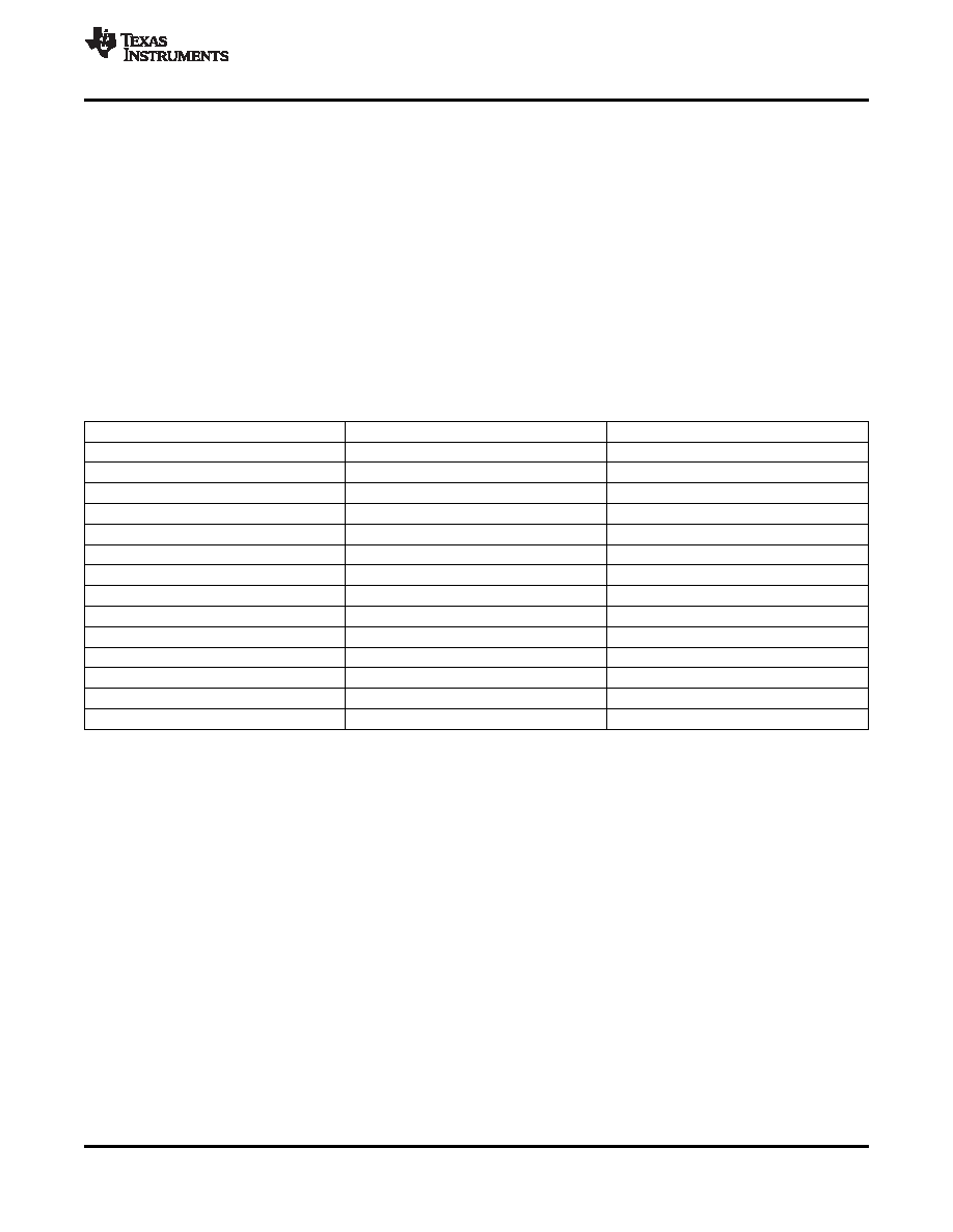
Table 5. Single-Ended Input Impedance vs PGA Ranges (1)
Mixer Gain (dB)
Microphone PGA Range (dB)
Input Impedance (
Ω)
0
–5.5
35,000
0
6
–11.5
38,889
0
12
–17.5
42,000
0
18
–23.5
44,074
0
24
–29.5
45,294
0
30
–35.5
45,960
0
36
–40
46,308
–6
0
–5.5
62,222
–6
6
–11.5
70,000
–6
12
–17.5
77,778
–6
18
–23.5
84,000
–6
24
–29.5
88,148
–6
30
–35.5
90,588
–6
36
–40
91,919
(1)
Valid when only one input is enabled
MICBIAS GENERATION
The TLV320ADC3001 includes a programmable microphone bias output voltage (MICBIAS), capable of providing
output voltages of 2 V or 2.5 V (both derived from the on-chip band-gap voltage) with 4-mA output-current drive
capability. In addition, the MICBIAS may be programmed to be switched to AVDD directly through an on-chip
switch, or it can be powered down completely when not needed, for power savings. This function is controlled by
register programming in page 1 / register 51.
ADC Decimation Filtering and Signal Processing
The TLV320ADC3001 ADC channel includes a built-in digital decimation filter to process the oversampled data
from the delta-sigma modulator to generate digital data at the Nyquist sampling rate with high dynamic range.
The decimation filter can be chosen from three different types, depending on the required frequency response,
group delay, and sampling rate.
Processing Blocks
The TLV320ADC3001 offers a range of processing blocks which implement various signal processing capabilities
along with decimation filtering. These processing blocks give users the choice of how much and what type of
signal processing they may use and which decimation filter is applied.
Copyright
2008–2011, Texas Instruments Incorporated
31
相關PDF資料 |
PDF描述 |
|---|---|
| TLV320ADC3001IYZHR | 2-CH 16-BIT PROPRIETARY METHOD ADC, SERIAL ACCESS, PBGA16 |
| TLV320ADC3101IRGER320 | SPECIALTY CONSUMER CIRCUIT, PQCC24 |
| TLV320ADC3101IRGET320 | SPECIALTY CONSUMER CIRCUIT, PQCC24 |
| TLV320ADC3101IRGER | SPECIALTY CONSUMER CIRCUIT, PQCC24 |
| TLV320ADC3101IRGET | SPECIALTY CONSUMER CIRCUIT, PQCC24 |
相關代理商/技術參數 |
參數描述 |
|---|---|
| TLV320ADC3001IYZHT | 制造商:Texas Instruments 功能描述:Analog/Digital (A/D) Converter IC |
| TLV320ADC3101 | 制造商:TI 制造商全稱:Texas Instruments 功能描述:Low Power Stereo ADC for Wireless Handsets and Portable Audio |
| TLV320ADC3101EVM-K | 功能描述:音頻 IC 開發工具 TLV320ADC3101EVM-K Eval Mod RoHS:否 制造商:Texas Instruments 產品:Evaluation Kits 類型:Audio Amplifiers 工具用于評估:TAS5614L 工作電源電壓:12 V to 38 V |
| TLV320ADC3101IRGER | 功能描述:音頻模/數轉換器 IC 92dB (16B) Low Power Stereo ADC RoHS:否 制造商:Wolfson Microelectronics 轉換速率: 分辨率: ADC 輸入端數量: 工作電源電壓: 最大工作溫度: 最小工作溫度: 安裝風格: 封裝 / 箱體: 封裝: |
| TLV320ADC3101IRGET | 功能描述:音頻模/數轉換器 IC 92dB (16B) Low Power Stereo ADC RoHS:否 制造商:Wolfson Microelectronics 轉換速率: 分辨率: ADC 輸入端數量: 工作電源電壓: 最大工作溫度: 最小工作溫度: 安裝風格: 封裝 / 箱體: 封裝: |
發布緊急采購,3分鐘左右您將得到回復。