- 您現(xiàn)在的位置:買賣IC網(wǎng) > PDF目錄98285 > TPS65200YFFR (TEXAS INSTRUMENTS INC) 1-CHANNEL POWER SUPPLY SUPPORT CKT, BGA36 PDF資料下載
參數(shù)資料
| 型號: | TPS65200YFFR |
| 廠商: | TEXAS INSTRUMENTS INC |
| 元件分類: | 電源管理 |
| 英文描述: | 1-CHANNEL POWER SUPPLY SUPPORT CKT, BGA36 |
| 封裝: | 2.80 X 2.60 MM, 0.40 MM PITCH, GREEN, DSBGA-36 |
| 文件頁數(shù): | 58/59頁 |
| 文件大小: | 2424K |
| 代理商: | TPS65200YFFR |
第1頁第2頁第3頁第4頁第5頁第6頁第7頁第8頁第9頁第10頁第11頁第12頁第13頁第14頁第15頁第16頁第17頁第18頁第19頁第20頁第21頁第22頁第23頁第24頁第25頁第26頁第27頁第28頁第29頁第30頁第31頁第32頁第33頁第34頁第35頁第36頁第37頁第38頁第39頁第40頁第41頁第42頁第43頁第44頁第45頁第46頁第47頁第48頁第49頁第50頁第51頁第52頁第53頁第54頁第55頁第56頁第57頁當(dāng)前第58頁第59頁
SLVSA48 – APRIL 2010
www.ti.com
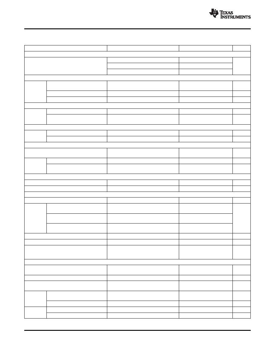
ELECTRICAL CHARACTERISTICS (continued)
VBAT = 3.6 V ±5%, TJ = 27C (unless otherwise noted)
PARAMETER
TEST CONDITIONS
MIN
TYP
MAX
UNIT
INPUT CURRENT LIMITING
IIN_LIMIT = 100 mA
88
93
98
IIN_LIMIT
Input current limiting threshold
IIN_LIMIT = 500 mA
450
475
500
mA
IIN_LIMIT = 975 mA
875
925
975
VDD REGULATOR
VBUS > VIN(min) or VSYS > VBATMIN,
Internal bias regulator voltage
2
6.5
V
IVDD = 1 mA, CVDD = 1 mF
VDD
VDD output short current limit
30
mA
Voltage from BST pin to SWC pin
During charge or boost operation
6.5
V
BATTERY RECHARGE THRESHOLD
Recharge threshold voltage
Below VOREG
100
130
160
mV
VRCH
VCSOUT decreasing below threshold,
Deglitch time
130
ms
tFALL = 100 ns, 10-mV overdrive
STAT OUTPUT
Low-level output saturation voltage
IO = 10 mA, sink current
0.4
V
VOL(STAT)
High-level leakage current
Voltage on STAT pin is 5 V
1
A
REVERSE PROTECTION COMPARATOR
Reverse protection threshold,
VREV
2.3 V
≤ VCSOUT ≤ VOREG, VBUS falling
0
40
100
mV
VBUS-VCSOUT
Reverse protection exit hysteresis
2.3 V
≤ VCSOUT ≤ VOREG
140
200
260
mV
VREV-EXIT
Deglitch time for VBUS rising above
Rising voltage
30
ms
VREV + VREV_EXIT
VBUS UVLO
VUVLO
IC active threshold voltage
VBUS rising
3.05
3.3
3.55
V
VUVLO_HYS
IC active hysteresis
VBUS falling from above VUVLO
120
150
mV
PWM
fPWM
PWM frequency, charger
3
MHz
Internal top reverse blocking
IIN_LIMIT = 500 mA,
180
MOSFET on-resistance
Measured from VBUS to PMID
Internal top N-channel Switching
RDSON
Measured from PMID to SWC
120
m
Ω
MOSFET on-resistance
Internal bottom N-channel
Measured from SW to PGND
150
MOSFET on-resistance
DMAX
Maximum duty cycle
99.5
%
DMIN
Minimum duty cycle
0
%
Synchronous mode to
Low-side MOSFET
nonsynchronous mode transition
100
mA
cycle-by-cycle current sensing
current threshold(1)
BOOST MODE OPERATION FOR VBUS (OPA_MODE=1, HZ_MODE=0)
2.5 V < VBUS < 4.5 V; Including line and
VBUS_B
Boost output voltage (to pin VBUS)
4.75
5
5.25
V
load regulation over full temp range
IBO
Maximum output current for boost
VBUS_B = 5 V, 2.5 V < VBUS < 4.5 V
200
mA
Cycle by cycle current limit for
IBLIMIT
VBUS_B = 5 V, 2.5 V < VSYS < 4.5 V
1
A
boost
Over voltage protection threshold
Threshold over VBUS to turn off converter
5.8
6
6.2
V
for boost (VBUS pin)
during boost
VBUSOVP
VBUSOVP hysteresis
VBUS falling from above VBUSOVP
200
mV
Maximum battery voltage for boost
VSYS rising edge during boost
4.75
4.9
5.05
V
VBATMAX
VBATMAX hysteresis
VSYS falling from above VBATMAX
200
mV
(1)
Bottom N-channel MOSFET always turns on for ~60 ns and then turns off if current is too low.
8
Copyright 2010, Texas Instruments Incorporated
Product Folder Link(s): TPS65200
相關(guān)PDF資料 |
PDF描述 |
|---|---|
| TPS65251RHAT | SWITCHING REGULATOR, PQCC40 |
| TPS65251RHAR | SWITCHING REGULATOR, PQCC40 |
| TPS65257RHAT | 4 A SWITCHING REGULATOR, 2200 kHz SWITCHING FREQ-MAX, PQCC40 |
| TPS65510RGTRG4 | 1-CHANNEL POWER SUPPLY SUPPORT CKT, PQCC16 |
| TPS65510RGTTG4 | 1-CHANNEL POWER SUPPLY SUPPORT CKT, PQCC16 |
相關(guān)代理商/技術(shù)參數(shù) |
參數(shù)描述 |
|---|---|
| TPS65200YFFT | 功能描述:PMIC 解決方案 Li+ Batt Chrgr RoHS:否 制造商:Texas Instruments 安裝風(fēng)格:SMD/SMT 封裝 / 箱體:QFN-24 封裝:Reel |
| TPS65-201A-S | 功能描述:65MM RECTANGLE TRACKPAD 制造商:azoteq (pty) ltd 系列:IQ Switch?,ProxSense? 零件狀態(tài):在售 傳感器類型:電容性 輸出類型:數(shù)字 工作溫度:0°C ~ 40°C 標(biāo)準(zhǔn)包裝:1 |
| TPS65203YFFR | 制造商:TI 功能描述:Ox Low End |
| TPS65217AEVM | 功能描述:電源管理IC開發(fā)工具 TPS65217A Eval Mod RoHS:否 制造商:Maxim Integrated 產(chǎn)品:Evaluation Kits 類型:Battery Management 工具用于評估:MAX17710GB 輸入電壓: 輸出電壓:1.8 V |
| TPS65217ARSLR | 功能描述:PMIC 解決方案 Sgl Chip Pwr Sol RoHS:否 制造商:Texas Instruments 安裝風(fēng)格:SMD/SMT 封裝 / 箱體:QFN-24 封裝:Reel |
發(fā)布緊急采購,3分鐘左右您將得到回復(fù)。