- 您現在的位置:買賣IC網 > PDF目錄373914 > AD7707 (Analog Devices, Inc.) ECONOLINE: REC2.2-S_DR/H1 - 2.2W DIP Package- 1kVDC Isolation- Regulated Output- UL94V-0 Package Material- Continuous Short Circiut Protection- Internal SMD design- 100% Burned In- Efficiency to 75% PDF資料下載
參數資料
| 型號: | AD7707 |
| 廠商: | Analog Devices, Inc. |
| 英文描述: | ECONOLINE: REC2.2-S_DR/H1 - 2.2W DIP Package- 1kVDC Isolation- Regulated Output- UL94V-0 Package Material- Continuous Short Circiut Protection- Internal SMD design- 100% Burned In- Efficiency to 75% |
| 中文描述: | 3 V / 5號第五,1毫瓦3 -10 V輸入范圍通道16位Σ-Δ模數轉換器 |
| 文件頁數: | 17/40頁 |
| 文件大小: | 316K |
| 代理商: | AD7707 |
第1頁第2頁第3頁第4頁第5頁第6頁第7頁第8頁第9頁第10頁第11頁第12頁第13頁第14頁第15頁第16頁當前第17頁第18頁第19頁第20頁第21頁第22頁第23頁第24頁第25頁第26頁第27頁第28頁第29頁第30頁第31頁第32頁第33頁第34頁第35頁第36頁第37頁第38頁第39頁第40頁
REV. A
AD7707
–17–
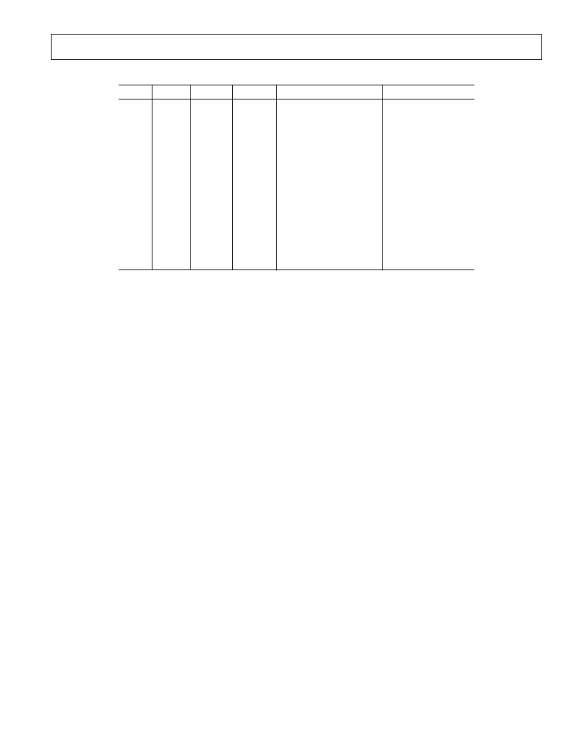
Table XIV. Output Update Rates
CLK*
FS2
FS1
FS0
Output Update Rate
–3 dB Filter Cutoff
0
0
0
0
1
1
1
1
0
0
0
0
1
1
1
1
0
0
0
0
0
0
0
0
1
1
1
1
1
1
1
1
0
0
1
1
0
0
1
1
0
0
1
1
0
0
1
1
0
1
0
1
0
1
0
1
0
1
0
1
0
1
0
1
20 Hz
25 Hz
100 Hz
200 Hz
50 Hz
60 Hz
250 Hz
500 Hz
4.054 Hz
4.23 Hz
4.84 Hz
4.96 Hz
10 Hz
10.34 Hz
11.90 Hz
12.2 Hz
5.24 Hz
6.55 Hz
26.2 Hz
52.4 Hz
13.1 Hz
15.7 Hz
65.5 Hz
131 Hz
1.06 Hz
1.11 Hz
1.27 Hz
1.3 Hz
2.62 Hz
2.71 Hz
3.13 Hz
3.2 Hz
*Assumes correct clock frequency on MCLK IN pin with CLKDIV bit set appropriately.
Data Register (RS2, RS1, RS0 = 0, 1, 1)
The Data Register on the part is a 16-bit read-only register that contains the most up-to-date conversion result from the AD7707. If
the Communications Register sets up the part for a write operation to this register, a write operation must actually take place to re-
turn the part to where it is expecting a write operation to the Communications Register. However, the 16 bits of data written to the
part will be ignored by the AD7707.
Test Register (RS2, RS1, RS0 = 1, 0, 0); Power-On/Reset Status: 00Hex
The part contains a Test Register that is used when testing the device. The user is advised not to change the status of any of the bits
in this register from the default (Power-on or
RESET
) status of all 0s as the part will be placed in one of its test modes and will not
operate correctly.
Zero-Scale Calibration Register (RS2, RS1, RS0 = 1, 1, 0); Power-On/Reset Status: 1F4000Hex
The AD7707 contains independent sets of zero-scale registers, one for each of the input channels. Each of these registers is a 24-bit
read/write register; 24 bits of data must be written otherwise no data will be transferred to the register. This register is used in con-
junction with its associated full-scale register to form a register pair. These register pairs are associated with input channel pairs as
outlined in Table VII. While the part is set up to allow access to these registers over the digital interface, the part itself no longer has
access to the register coefficients to correctly scale the output data. As a result, there is a possibility that after accessing the calibra-
tion registers (either read or write operation) the first output data read from the part may contain incorrect data. In addition, a write
to the calibration register should not be attempted while a calibration is in progress. These eventualities can be avoided by taking the
FSYNC bit in the mode register high before the calibration register operation and taking it low after the operation is complete.
Full-Scale Calibration Register (RS2, RS1, RS0 = 1, 1, 1); Power-On/Reset Status: 5761ABHex
The AD7707 contains independent sets of full-scale registers, one for each of the input channels. Each of these registers is a 24-bit
read/write register; 24 bits of data must be written otherwise no data will be transferred to the register. This register is used in con-
junction with its associated zero-scale register to form a register pair. These register pairs are associated with input channel pairs as
outlined in Table X. While the part is set up to allow access to these registers over the digital interface, the part itself no longer has
access to the register coefficients to correctly scale the output data. As a result, there is a possibility that after accessing the calibra-
tion registers (either read or write operation) the first output data read from the part may contain incorrect data. In addition, a write
to the calibration register should not be attempted while a calibration is in progress. These eventualities can be avoided by taking
FSYNC bit in the mode register high before the calibration register operation and taking it low after the operation is complete.
相關PDF資料 |
PDF描述 |
|---|---|
| AD7707EB | 3 V/5 V 610 V Input Range 1 mW 3-Channel 16-Bit Sigma-Delta ADC(316.51 k) |
| AD7708BR | Shaft; Style: 2 - light; Applicable Model: LE-P / LEL-W |
| AD7708BRU | 8-/10-Channel, Low Voltage, Low Power, ADCs |
| AD7708 | 8-/10-Channel, Low Voltage, Low Power, ADCs |
| AD7718 | 8-/10-Channel, Low Voltage, Low Power, ADCs |
相關代理商/技術參數 |
參數描述 |
|---|---|
| AD7707BR | 功能描述:IC ADC 16BIT 3CH 20-SOIC RoHS:否 類別:集成電路 (IC) >> 數據采集 - 模數轉換器 系列:- 標準包裝:1,000 系列:- 位數:12 采樣率(每秒):300k 數據接口:并聯 轉換器數目:1 功率耗散(最大):75mW 電壓電源:單電源 工作溫度:0°C ~ 70°C 安裝類型:表面貼裝 封裝/外殼:24-SOIC(0.295",7.50mm 寬) 供應商設備封裝:24-SOIC 包裝:帶卷 (TR) 輸入數目和類型:1 個單端,單極;1 個單端,雙極 |
| AD7707BR-REEL | 制造商:Analog Devices 功能描述:ADC Single Delta-Sigma 500sps 16-bit Serial 20-Pin SOIC W T/R 制造商:Analog Devices 功能描述:ADC SGL DELTA-SIGMA 0.5KSPS 16BIT SERL 20SOIC W - Tape and Reel |
| AD7707BR-REEL7 | 制造商:Analog Devices 功能描述:ADC Single Delta-Sigma 500sps 16-bit Serial 20-Pin SOIC W T/R 制造商:Analog Devices 功能描述:ADC SGL DELTA-SIGMA 0.5KSPS 16BIT SERL 20SOIC W - Tape and Reel |
| AD7707BRU | 功能描述:IC ADC 16BIT 3CH 20-TSSOP RoHS:否 類別:集成電路 (IC) >> 數據采集 - 模數轉換器 系列:- 標準包裝:1,000 系列:- 位數:12 采樣率(每秒):300k 數據接口:并聯 轉換器數目:1 功率耗散(最大):75mW 電壓電源:單電源 工作溫度:0°C ~ 70°C 安裝類型:表面貼裝 封裝/外殼:24-SOIC(0.295",7.50mm 寬) 供應商設備封裝:24-SOIC 包裝:帶卷 (TR) 輸入數目和類型:1 個單端,單極;1 個單端,雙極 |
| AD7707BRU-REEL | 制造商:Analog Devices 功能描述:ADC Single Delta-Sigma 500sps 16-bit Serial 20-Pin TSSOP T/R 制造商:Analog Devices 功能描述:ADC SGL DELTA-SIGMA 0.5KSPS 16BIT SERL 20TSSOP - Tape and Reel |
發布緊急采購,3分鐘左右您將得到回復。