- 您現在的位置:買賣IC網 > PDF目錄373914 > AD7713SQ (ANALOG DEVICES INC) LC2MOS Loop-Powered Signal Conditioning ADC PDF資料下載
參數資料
| 型號: | AD7713SQ |
| 廠商: | ANALOG DEVICES INC |
| 元件分類: | ADC |
| 英文描述: | LC2MOS Loop-Powered Signal Conditioning ADC |
| 中文描述: | 3-CH 24-BIT DELTA-SIGMA ADC, SERIAL ACCESS, CDIP24 |
| 封裝: | 0.300 INCH, HERMETIC SEALED, CERDIP-24 |
| 文件頁數: | 15/28頁 |
| 文件大小: | 516K |
| 代理商: | AD7713SQ |
第1頁第2頁第3頁第4頁第5頁第6頁第7頁第8頁第9頁第10頁第11頁第12頁第13頁第14頁當前第15頁第16頁第17頁第18頁第19頁第20頁第21頁第22頁第23頁第24頁第25頁第26頁第27頁第28頁
2
–15–
REV. C
AD7713
introduced on the analog inputs. Both inputs of the differential
input channels look into similar input circuitry.
In any case, the error introduced due to longer charging times is
a gain error which can be removed using the system calibration
capabilities of the AD7713 provided that the resultant span is
within the span limits of the system calibration techniques for
the AD7713.
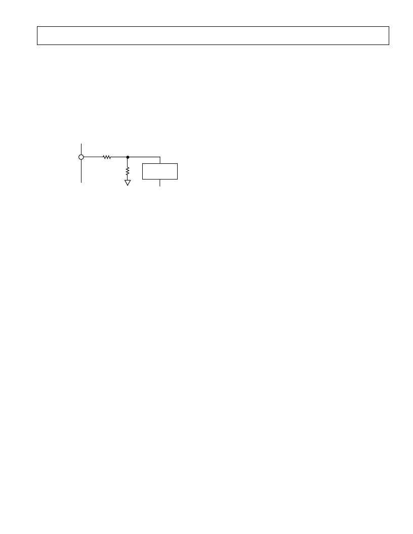
The AIN3 input contains a resistive attenuation network as out-
lined in Figure 8. The typical input impedance on this input is
44 k
. As a result, the AIN3 input should be driven from a low
impedance source.
AIN3
33k
11k
V
BIAS
MODULATOR
CIRCUIT
Figure 8. AIN3 Input Impedance
ANALOG INPUT FUNCTIONS
Analog Input Ranges
The analog inputs on the AD7713 provide the user with consid-
erable flexibility in terms of analog input voltage ranges. Two of
the inputs are differential, programmable-gain, input channels
which can handle either unipolar or bipolar input signals. The
common-mode range of these inputs is from AGND to AV
DD
provided that the absolute value of the analog input voltage lies
between AGND – 30 mV and AV
DD
+ 30 mV. The third analog
input is a single-ended, programmable gain high-level input
which accepts analog input ranges of 0 to +4
×
V
REF
/GAIN.
The dc input leakage current on the AIN1 and AIN2 inputs is
10 pA maximum at 25
°
C (
±
1 nA over temperature). This results
in a dc offset voltage developed across the source impedance.
However, this dc offset effect can be compensated for by a com-
bination of the differential input capability of the part and its
system calibration mode. The dc input current on the AIN3 in-
put depends on the input voltage. For the nominal input voltage
range of +10 V, the input current is 225
μ
A typ.
Burn Out Current
The AIN1(+) input of the AD7713 contains a 1
μ
A current
source which can be turned on/off via the control register. This
current source can be used in checking that a transducer has not
burnt out or gone open circuit before attempting to take mea-
surements on that channel. If the current is turned on and is al-
lowed flow into the transducer and a measurement of the input
voltage on the AIN1 input is taken, it can indicate that the
transducer is not functioning correctly. For normal operation,
this burn out current is turned off by writing a 0 to the BO bit in
the control register.
RTD Excitation Currents
The AD7713 also contains two matched 200
μ
A constant cur-
rent sources which are provided at the RTD1 and RTD2 pins of
the device. These currents can be turned on/off via the control
register. Writing a 1 to the RO bit of the control register enables
these excitation currents.
For four-wire RTD applications, one of these excitation cur-
rents is used to provide the excitation current for the RTD; the
second current source can be left unconnected. For three-wire
RTD configurations, the second on-chip current source can be
used to eliminate errors due to voltage drops across lead resis-
tances. Figures 20 and 21 in the Application section show some
RTD configurations with the AD7713.
The temperature coefficient of the RTD current sources is typi-
cally 20 ppm/
°
C with a typical matching between the tempera-
ture coefficients of both current sources of 3 ppm/
°
C. For
applications where the absolute value of the temperature coeffi-
cient is too large, the following schemes can be used to remove
the drift error.
The conversion result from the AD7713 is ratiometric to the
V
REF
voltage. Therefore, if the V
REF
voltage varies with the RTD
temperature coefficient, the temperature drift from the current
source will be removed. For four-wire RTD applications, the
reference voltage can be made ratiometric to RTD current
source by using the second current with a low TC resistor to
generate the reference voltage for the part. In this case if a
12.5 k
resistor is used, the 200
μ
A current source generates
+2.5 V across the resistor. This +2.5 V can be applied to the
REF IN(+) input of the AD7713 and the REF IN(–) input at
ground it will supply a V
REF
of 2.5 V for the part. For three-wire
RTD configurations, the reference voltage for the part is gener-
ated by placing a low TC resistor (12.5 k
for 2.5 V reference)
in series with one of the constant current sources. The RTD
current sources can be driven to within 2 V of AV
DD
. The refer-
ence input of the AD7713 is differential so the REF IN(+) and
REF IN(–) of the AD7713 are driven from either side of the re-
sistor. Both schemes ensure that the reference voltage for the
part tracks the RTD current sources over temperature and,
thereby, removes the temperature drift error.
Bipolar/Unipolar Inputs
Two analog inputs on the AD7713 can accept either unipolar or
bipolar input voltage ranges while the third channel accepts only
unipolar signals. Bipolar or unipolar options for AIN1 and
AIN2 are chosen by programming the B/U bit of the control
register. This programs both channels for either unipolar or bi-
polar operation. Programming the part for either unipolar or
bipolar operation does not change any of the input signal condi-
tioning; it simply changes the data output coding. The data cod-
ing is binary for unipolar inputs and offset binary for bipolar
inputs.
The AIN1 and AIN2 input channels are differential, and as a
result, the voltage to which the unipolar and bipolar signals are
referenced is the voltage on the AIN1(–) and AIN2(–) inputs.
For example, if AIN1(–) is +1.25 V and the AD7713 is config-
ured for unipolar operation with a gain of 1 and a V
REF
of
+2.5 V, the input voltage range on the AIN1(+) input is
+1.25 V to +3.75 V. For the AIN3 input, the input signals are
referenced to AGND.
REFERENCE INPUT
The reference inputs of the AD7713, REF IN(+) and
REF IN(–) provide a differential reference input capability. The
common-mode range for these differential inputs is from V
SS
to
AV
DD
. The nominal differential voltage, V
REF
(REF IN(+) –
REF IN(–)), is +2.5 V for specified operation, but the reference
相關PDF資料 |
PDF描述 |
|---|---|
| AD7713 | Loop-Powered Signal Conditioning ADC(循環驅動LC2MOS信號調節A/D轉換器) |
| AD7714AN-3 | VARISTOR 30VRMS 0805 SMD |
| AD7714AN-5 | VARISTOR 40VRMS 1206 SMD |
| AD7714YRU | 3 V/5 V, CMOS, 500 uA Signal Conditioning ADC |
| AD7714* | 3 V/5 V. CMOS. 500 uA Signal Conditioning ADC |
相關代理商/技術參數 |
參數描述 |
|---|---|
| AD7714 | 制造商:AD 制造商全稱:Analog Devices 功能描述:3 V/5 V, CMOS, 500 uA Signal Conditioning ADC |
| AD7714ACHIPS-3 | 制造商:AD 制造商全稱:Analog Devices 功能描述:3 V/5 V, CMOS, 500 uA Signal Conditioning ADC |
| AD7714ACHIPS-5 | 制造商:AD 制造商全稱:Analog Devices 功能描述:3 V/5 V, CMOS, 500 uA Signal Conditioning ADC |
| AD7714AN-3 | 制造商:Rochester Electronics LLC 功能描述:24-BIT SIGMA DELTA A/D IC - Bulk 制造商:Analog Devices 功能描述: |
發布緊急采購,3分鐘左右您將得到回復。