- 您現在的位置:買賣IC網 > PDF目錄373914 > AD7713SQ (ANALOG DEVICES INC) LC2MOS Loop-Powered Signal Conditioning ADC PDF資料下載
參數資料
| 型號: | AD7713SQ |
| 廠商: | ANALOG DEVICES INC |
| 元件分類: | ADC |
| 英文描述: | LC2MOS Loop-Powered Signal Conditioning ADC |
| 中文描述: | 3-CH 24-BIT DELTA-SIGMA ADC, SERIAL ACCESS, CDIP24 |
| 封裝: | 0.300 INCH, HERMETIC SEALED, CERDIP-24 |
| 文件頁數: | 18/28頁 |
| 文件大小: | 516K |
| 代理商: | AD7713SQ |
第1頁第2頁第3頁第4頁第5頁第6頁第7頁第8頁第9頁第10頁第11頁第12頁第13頁第14頁第15頁第16頁第17頁當前第18頁第19頁第20頁第21頁第22頁第23頁第24頁第25頁第26頁第27頁第28頁
REV. C
–18–
AD7713
Table IV. Calibration Truth Table
Cal Type
MD2, MD1, MD0
Zero-Scale Cal
Full-Scale Cal
Sequence
Duration
Self-Cal
System Cal
System Cal
System Offset Cal
Background Cal
0, 0, 1
0, 1, 0
0, 1, 1
1, 0, 0
1, 0, 1
Shorted Inputs
AIN
V
REF
One Step
Two Step
Two Step
One Step
One Step
9
×
1/Output Rate
4
×
1/Output Rate
4
×
1/Output Rate
9
×
1/Output Rate
6
×
1/Output Rate
AIN
V
REF
V
REF
AIN
Shorted Inputs
Span and Offset Limits
Whenever a system calibration mode is used, there are limits on
the amount of offset and span that can be accommodated. The
range of input span in both the unipolar and bipolar modes for
AIN1 and AIN2 has a minimum value of 0.8
×
V
REF
/GAIN and
a maximum value of 2.1
×
V
REF
/GAIN. For AIN3, the mini-
mum value is 3.2
×
V
REF
/GAIN while the maximum value is
4.2
×
V
REF
/GAIN.
The amount of offset which can be accommodated depends on
whether the unipolar or bipolar mode is being used. This offset
range is limited by the requirement that the positive full-scale
calibration limit is
≤
1.05
×
V
REF
/GAIN for AIN1 and AIN2.
Therefore, the offset range plus the span range cannot exceed
1.05
×
V
REF
/GAIN for AIN1 and AIN2. If the span is at its
minimum (0.8
×
V
REF
/GAIN) the maximum the offset can be is
(0.25
×
V
REF
/GAIN) for AIN1 and AIN2. For AIN3, both
ranges are multiplied by a factor of four.
In the bipolar mode, the system offset calibration range is again
restricted by the span range. The span range of the converter in
bipolar mode is equidistant around the voltage used for the
zero-scale point, thus the offset range plus half the span range
cannot exceed (1.05
×
V
REF
/GAIN) for AIN1 and AIN2. If the
span is set to 2
×
V
REF
/GAIN, the offset span cannot move
more than
±
(0.05
×
V
REF
/GAIN) before the endpoints of the
transfer function exceed the input overrange limits
±
(1.05
×
V
REF
/GAIN) for AIN1. If the span range is set to the minimum
±
(0.4
×
V
REF
/GAIN), the maximum allowable offset range is
±
(0.65
×
V
REF
/GAIN) for AIN1 and AIN2. The AIN3 input can
only be used in the unipolar mode..
POWER-UP AND CALIBRATION
On power-up, the AD7713 performs an internal reset which sets
the contents of the control register to a known state. However,
to ensure correct calibration for the device a calibration routine
should be performed after power-up.
The power dissipation and temperature drift of the AD7713 are
low and no warm-up time is required before the initial calibra-
tion is performed. However, the external reference must have
stabilized before calibration is initiated.
Drift Considerations
The AD7713 uses chopper stabilization techniques to minimize
input offset drift. Charge injection in the analog switches and dc
leakage currents at the sampling node are the primary sources of
offset voltage drift in the converter. The dc input leakage cur-
rent is essentially independent of the selected gain. Gain drift
within the converter depends primarily upon the temperature
tracking of the internal capacitors. It is not affected by leakage
currents.
Measurement errors due to offset drift or gain drift can be elimi-
nated at any time by recalibrating the converter or by operating
the part in the background calibration mode. Using the system
calibration mode can also minimize offset and gain errors in the
signal conditioning circuitry. Integral and differential linearity
errors are not significantly affected by temperature changes.
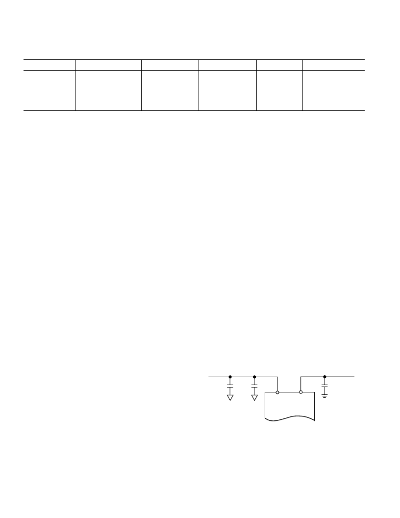
POWER SUPPLIES AND GROUNDING
The analog and digital supplies to the AD7713 are independent
and separately pinned out to minimize coupling between the
analog and digital sections of the device. The digital filter will
provide rejection of broadband noise on the power supplies, ex-
cept at integer multiples of the modulator sampling frequency.
The digital supply (DV
DD
) must not exceed the analog positive
supply (AV
DD
) by more than 0.3 V. If separate analog and digi-
tal supplies are used, the recommended decoupling scheme is
shown in Figure 9. In systems where AV
DD
= +5 V and DV
DD
=
+5 V, it is recommended that AV
DD
and DV
DD
are driven from
the same +5 V supply, although each supply should be de-
coupled separately as shown in Figure 9. It is preferable that the
common supply is the system’s analog +5 V supply.
It is also important that power is applied to the AD7713 before
signals at REF IN, AIN or the logic input pins in order to avoid
excessive current. If separate supplies are used for the AD7713
and the system digital circuitry, then the AD7713 should be
powered up first. If it is not possible to guarantee this, then cur-
rent limiting resistors should be placed in series with the logic
inputs.
AD7713
0.1μF
0.1μF
10μF
AV
DD
DV
DD
ANALOG
SUPPLY
DIGITAL +5V
SUPPLY
Figure 9. Recommended Decoupling Scheme
相關PDF資料 |
PDF描述 |
|---|---|
| AD7713 | Loop-Powered Signal Conditioning ADC(循環驅動LC2MOS信號調節A/D轉換器) |
| AD7714AN-3 | VARISTOR 30VRMS 0805 SMD |
| AD7714AN-5 | VARISTOR 40VRMS 1206 SMD |
| AD7714YRU | 3 V/5 V, CMOS, 500 uA Signal Conditioning ADC |
| AD7714* | 3 V/5 V. CMOS. 500 uA Signal Conditioning ADC |
相關代理商/技術參數 |
參數描述 |
|---|---|
| AD7714 | 制造商:AD 制造商全稱:Analog Devices 功能描述:3 V/5 V, CMOS, 500 uA Signal Conditioning ADC |
| AD7714ACHIPS-3 | 制造商:AD 制造商全稱:Analog Devices 功能描述:3 V/5 V, CMOS, 500 uA Signal Conditioning ADC |
| AD7714ACHIPS-5 | 制造商:AD 制造商全稱:Analog Devices 功能描述:3 V/5 V, CMOS, 500 uA Signal Conditioning ADC |
| AD7714AN-3 | 制造商:Rochester Electronics LLC 功能描述:24-BIT SIGMA DELTA A/D IC - Bulk 制造商:Analog Devices 功能描述: |
發布緊急采購,3分鐘左右您將得到回復。