- 您現在的位置:買賣IC網 > PDF目錄373914 > AD7713SQ (ANALOG DEVICES INC) LC2MOS Loop-Powered Signal Conditioning ADC PDF資料下載
參數資料
| 型號: | AD7713SQ |
| 廠商: | ANALOG DEVICES INC |
| 元件分類: | ADC |
| 英文描述: | LC2MOS Loop-Powered Signal Conditioning ADC |
| 中文描述: | 3-CH 24-BIT DELTA-SIGMA ADC, SERIAL ACCESS, CDIP24 |
| 封裝: | 0.300 INCH, HERMETIC SEALED, CERDIP-24 |
| 文件頁數: | 24/28頁 |
| 文件大?。?/td> | 516K |
| 代理商: | AD7713SQ |
第1頁第2頁第3頁第4頁第5頁第6頁第7頁第8頁第9頁第10頁第11頁第12頁第13頁第14頁第15頁第16頁第17頁第18頁第19頁第20頁第21頁第22頁第23頁當前第24頁第25頁第26頁第27頁第28頁
REV. C
–24–
AD7713
which is in its single chip mode. The
DRDY
line from the
AD7713 is connected to the Port PC0 input of the 68HC11 so
the
DRDY
line is polled by the 68HC11. The
DRDY
line can
be connected to the
IRQ
input of the 68HC11 if an interrupt
driven system is preferred. The 68HC11 MOSI and MISO lines
should be configured for wired-or operation. Depending on the
interface configuration, it may be necessary to provide bidirec-
tional buffers between the 68HC11’s MOSI and MISO lines.
The 68HC11 is configured in the master mode with its CPOL
bit set to a logic zero and its CPHA bit set to a logic one.
DV
DD
SYNC
RFS
TFS
A0
SDATA
SCLK
MODE
PC0
PC1
PC2
PC3
MISO
MOSI
68HC11
AD7713
DRDY
SS
SCK
DV
DD
Figure 18. AD7713 to 68HC11 Interface
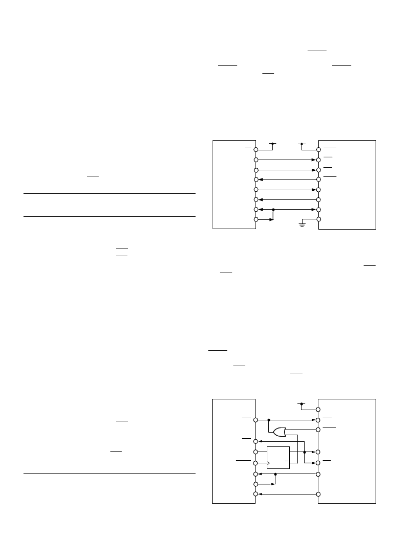
AD7713 to ADSP-2105 Interface
An interface circuit between the AD7713 and the ADSP-2105
microprocessor is shown in Figure 19. In this interface, the
AD7713 is configured for its self-clocking mode while the
RFS
and
TFS
pins of the ADSP-2105 are configured as inputs and
the ADSP-2105 serial clock line is also configured as an input.
When the ADSP-2105’s serial clock is configured as an input it
needs a couple of clock pulses to initialize itself correctly before
accepting data. Therefore, the first read from the AD7713 may
not read correct data. In the interface shown, a read operation
to the AD7713 accesses either the output register or the calibra-
tion registers. Data cannot be read from the control register. A
write operation always writes to the control or calibration
registers.
DRDY
is used as the frame synchronization pulse for read op-
erations from the output register and it is decoded with A0 to
drive the
RFS
inputs of both the AD7713 and the ADSP-2105.
The latched A0 line drives the
TFS
inputs of both the AD7713
and the ADSP-2105 as well as the AD7713 A0 input.
DV
DD
A0
SDATA
SCLK
MODE
A0
DR
ADSP-2105
AD7713
RFS
TFS
DRDY
RFS
TFS
74HC74
Q
D
Q
DT
SCLK
DMWR
Figure 19. AD7713 to ADSP-2105 Interface
READ 1:
MOV A,SBUF;
RLC A;
MOV B.0,C;
RLC A; MOV B.1,C; RLC A; MOV B.2,C;
RLC A; MOV B.3,C; RLC A; MOV B.4,C;
RLC A; MOV B.5,C; RLC A; MOV B.6,C;
RLC A; MOV B.7,C;
MOV A,B;
MOV @R0,A; Write Data to Memory
INC R0;
Increment Memory Location
DEC R1
Decrement Byte Counter
MOV A,R1
JZ END
Jump if Zero
JMP WAIT
Fetch Next Byte
END:
SETB 90H
Bring RFS High
FIN:
SJMP FIN
Read Buffer
Rearrange Data
Reverse Order of Bits
Table VI. 8XC51 Code for Writing to the AD7713
MOV SCON,#00000000B;
Configure 8051 for MODE 0
Operation & Enable Serial Reception
Enable Transmit Interrupt
Prioritize the Transmit Interrupt
Bring
TFS
High
Bring
RFS
High
Sets Number of Bytes to Be Written
in a Write Operation
Start Address in RAM for Bytes
Clear Accumulator
Initialize the Serial Port
MOV IE,#10010000B;
MOV IP,#00010000B;
SETB 91H;
SETB 90H;
MOV R1,#003H;
MOV R0,#030H;
MOV A,#00H;
MOV SBUF,A;
WAIT:
JMP WAIT;
INT ROUTINE:
NOP;
MOV A,R1;
JZ FIN;
DEC R1;
MOV A,@R;
INC R0;
RLC A;
Wait for Interrupt
Interrupt Subroutine
Load R1 to Accumulator
If Zero Jump to FIN
Decrement R1 Byte Counter
Move Byte into the Accumulator
Increment Address
Rearrange Data—From LSB First
to MSB First
MOV B.0,C; RLC A; MOV B.1,C; RLC A;
MOV B.2,C; RLC A; MOV B.3,C; RLC A;
MOV B.4,C; RLC A; MOV B.5,C; RLC A;
MOV B.6,C; RLC A: MOV B.7,C; MOV A,B;
CLR 93H;
CLR 91H;
MOV SBUF,A;
RETI;
FIN:
SETB 91H;
SETB 93H;
RETI;
Bring A0 Low
Bring
TFS
Low
Write to Serial Port
Return from Subroutine
Set
TFS
High
Set A0 High
Return from Interrupt Subroutine
AD7713 to 68HC11 Interface
Figure 18 shows an interface between the AD7713 and the
68HC11 microcontroller. The AD7713 is configured for its ex-
ternal clocking mode while the SPI port is used on the 68HC11
相關PDF資料 |
PDF描述 |
|---|---|
| AD7713 | Loop-Powered Signal Conditioning ADC(循環驅動LC2MOS信號調節A/D轉換器) |
| AD7714AN-3 | VARISTOR 30VRMS 0805 SMD |
| AD7714AN-5 | VARISTOR 40VRMS 1206 SMD |
| AD7714YRU | 3 V/5 V, CMOS, 500 uA Signal Conditioning ADC |
| AD7714* | 3 V/5 V. CMOS. 500 uA Signal Conditioning ADC |
相關代理商/技術參數 |
參數描述 |
|---|---|
| AD7714 | 制造商:AD 制造商全稱:Analog Devices 功能描述:3 V/5 V, CMOS, 500 uA Signal Conditioning ADC |
| AD7714ACHIPS-3 | 制造商:AD 制造商全稱:Analog Devices 功能描述:3 V/5 V, CMOS, 500 uA Signal Conditioning ADC |
| AD7714ACHIPS-5 | 制造商:AD 制造商全稱:Analog Devices 功能描述:3 V/5 V, CMOS, 500 uA Signal Conditioning ADC |
| AD7714AN-3 | 制造商:Rochester Electronics LLC 功能描述:24-BIT SIGMA DELTA A/D IC - Bulk 制造商:Analog Devices 功能描述: |
發布緊急采購,3分鐘左右您將得到回復。