- 您現在的位置:買賣IC網 > PDF目錄373914 > AD7713SQ (ANALOG DEVICES INC) LC2MOS Loop-Powered Signal Conditioning ADC PDF資料下載
參數資料
| 型號: | AD7713SQ |
| 廠商: | ANALOG DEVICES INC |
| 元件分類: | ADC |
| 英文描述: | LC2MOS Loop-Powered Signal Conditioning ADC |
| 中文描述: | 3-CH 24-BIT DELTA-SIGMA ADC, SERIAL ACCESS, CDIP24 |
| 封裝: | 0.300 INCH, HERMETIC SEALED, CERDIP-24 |
| 文件頁數: | 21/28頁 |
| 文件大小: | 516K |
| 代理商: | AD7713SQ |
第1頁第2頁第3頁第4頁第5頁第6頁第7頁第8頁第9頁第10頁第11頁第12頁第13頁第14頁第15頁第16頁第17頁第18頁第19頁第20頁當前第21頁第22頁第23頁第24頁第25頁第26頁第27頁第28頁
2
–21–
REV. C
AD7713
SDATA (O)
SCLK (I)
3-STATE
RFS (I)
A0 (I)
t
22
MSB
LSB
DRDY (O)
t
21
t
20
t
23
t
26
t
29
t
28
t
27
t
25
t
24
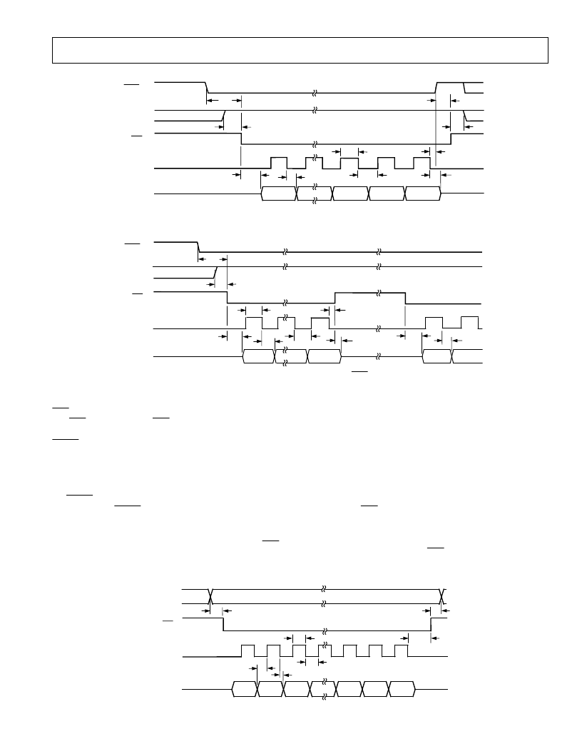
Figure 12a. External Clocking Mode, Output Data Read Operation
3-STATE
MSB
BIT N
BIT N+1
SDATA (O)
SCLK (I)
RFS (I)
A0 (I)
DRDY (O)
t
22
t
20
t
31
t
26
t
24
t
25
t
27
t
30
t
24
t
25
Figure 12b. External Clocking Mode, Output Data Read Operation (
RFS
Returns High During Read Operation)
RFS
, the next bit (BIT N + 1) may appear on the databus be-
fore
RFS
goes high. When
RFS
returns low again, it activates
the SDATA output. When the entire word is transmitted, the
DRDY
line will go high, turning off the SDATA output as per
Figure 12a.
Write Operation
Data can be written to either the control register or calibration
registers. In either case, the write operation is not affected by
the
DRDY
line, and the write operation does not have any effect
on the status of
DRDY
. A write operation to the control regis-
ter or the calibration register must always write 24 bits to the re-
spective register.
Figure 13a shows a write operation to the AD7713 with
TFS
remaining low for the duration of the write operation. A0 deter-
mines whether a write operation transfers data to the control
register or to the calibration registers. This A0 signal must
remain valid for the duration of the serial write operation. As
before, the serial clock line should be low between read and
write operations. The serial data to be loaded to the AD7713
must be valid on the high level of the externally applied SCLK
signal. Data is clocked into the AD7713 on the high level of this
SCLK signal with the MSB transferred first. On the last active
high time of SCLK, the LSB is loaded to the AD7713.
Figure 13b shows a timing diagram for a write operation to the
AD7713 with
TFS
returning high during the write operation
and returning low again to write the rest of the data word. Tim-
ing parameters and functions are very similar to that outlined for
Figure 13a, but Figure 13b has a number of additional times to
show timing relationships when
TFS
returns high in the middle
of transferring a word.
SCLK (I)
SDATA (I)
TFS (I)
A0 (I)
MSB
LSB
t
32
t
33
t
34
t
26
t
27
t
36
t
35
Figure 13a. External Clocking Mode, Control/Calibration Register Write Operation
相關PDF資料 |
PDF描述 |
|---|---|
| AD7713 | Loop-Powered Signal Conditioning ADC(循環驅動LC2MOS信號調節A/D轉換器) |
| AD7714AN-3 | VARISTOR 30VRMS 0805 SMD |
| AD7714AN-5 | VARISTOR 40VRMS 1206 SMD |
| AD7714YRU | 3 V/5 V, CMOS, 500 uA Signal Conditioning ADC |
| AD7714* | 3 V/5 V. CMOS. 500 uA Signal Conditioning ADC |
相關代理商/技術參數 |
參數描述 |
|---|---|
| AD7714 | 制造商:AD 制造商全稱:Analog Devices 功能描述:3 V/5 V, CMOS, 500 uA Signal Conditioning ADC |
| AD7714ACHIPS-3 | 制造商:AD 制造商全稱:Analog Devices 功能描述:3 V/5 V, CMOS, 500 uA Signal Conditioning ADC |
| AD7714ACHIPS-5 | 制造商:AD 制造商全稱:Analog Devices 功能描述:3 V/5 V, CMOS, 500 uA Signal Conditioning ADC |
| AD7714AN-3 | 制造商:Rochester Electronics LLC 功能描述:24-BIT SIGMA DELTA A/D IC - Bulk 制造商:Analog Devices 功能描述: |
發布緊急采購,3分鐘左右您將得到回復。