- 您現在的位置:買賣IC網 > PDF目錄373915 > AD7722AS (ANALOG DEVICES INC) 16-Bit, 195 kSPS CMOS, Sigma-Delta ADC PDF資料下載
參數資料
| 型號: | AD7722AS |
| 廠商: | ANALOG DEVICES INC |
| 元件分類: | ADC |
| 英文描述: | 16-Bit, 195 kSPS CMOS, Sigma-Delta ADC |
| 中文描述: | 1-CH 16-BIT DELTA-SIGMA ADC, SERIAL/PARALLEL ACCESS, PQFP44 |
| 封裝: | MS-022AA, MQFP-44 |
| 文件頁數: | 14/24頁 |
| 文件大小: | 526K |
| 代理商: | AD7722AS |
AD7722
–14–
REV. 0
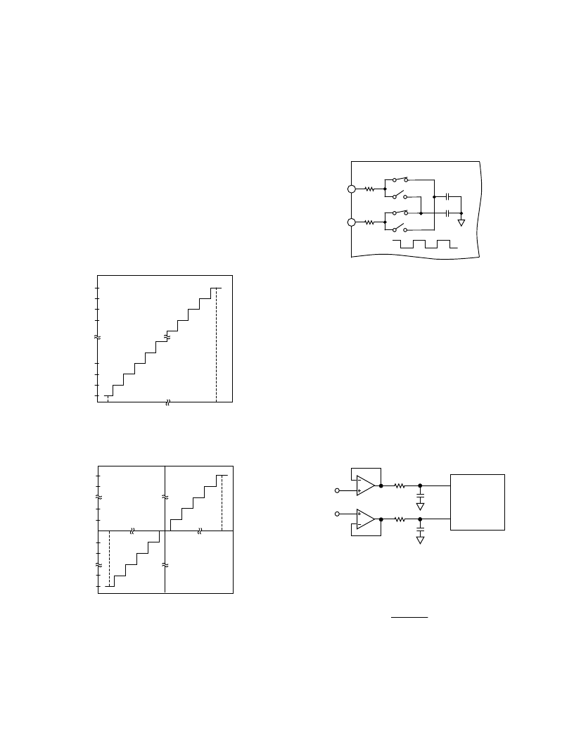
APPLYING THE AD7722
Analog Input Range
The AD7722 uses differential inputs to provide common-mode
noise rejection (i.e., the converted result will correspond to the
differential voltage between the two inputs). The absolute
voltage on both inputs must lie between AGND and AV
DD
.
In the unipolar mode, the full-scale analog input range (VIN(+)
– VIN(–)) is 0 V to V
REF2
. The output code is straight binary in
the unipolar mode with 1 LSB = 38
μ
V. The ideal transfer
function is shown in Figure 26.
In bipolar mode, the full-scale input range is
±
V
REF2
/2. The
bipolar mode allows complementary input signals. As another
example, in bipolar mode, VIN(–) can be connected to a dc bias
voltage to allow a single-ended input on VIN(+) equal to V
BIAS
±
V
REF2
/2. In bipolar mode the output code is 2s complement
with 1 LSB = 38
μ
V. The ideal transfer function is shown in
Figure 27.
111...111
111...110
111...101
111...100
000...011
000...010
000...001
000...000
OUTPUT
CODE
0V
V
–1LSB
DIFFERENTIAL INPUT VOLTAGE VIN(+) – VIN(–)
Figure 26. Unipolar Mode Transfer Function
111...111
111...110
100...001
100...000
000...010
000...001
000...000
OUTPUT
CODE
0V
+V
REF2
/2–1LSB
DIFFERENTIAL INPUT VOLTAGE VIN(+) – VIN(–)
–V
REF2
011...111
011...110
Figure 27. Bipolar Mode Transfer Function
Differential Inputs
The analog input to the modulator is a switched capacitor
design. The analog signal is converted into charge by highly
linear sampling capacitors. A simplified equivalent circuit
diagram of the analog input is shown in Figure 28. A signal
source driving the analog input must be able to provide the
charge onto the sampling capacitors every half CLKIN cycle
and settle to the required accuracy within the next half cycle.
18
Φ
A
Φ
B
Φ
A
Φ
B
16
2pF
2pF
AC
GROUND
500
Φ
A
Φ
B
Φ
A
Φ
B
CLKIN
VIN(+)
VIN(–)
AD7722
500
Figure 28. Analog Input Equivalent Circuit
Since the AD7722 samples the differential voltage across its
analog inputs, low noise performance is attained with an input
circuit that provides low common-mode noise at each input.
The amplifiers used to drive the analog inputs play a critical role
in attaining the high performance available from the AD7722.
When a capacitive load is switched onto the output of an op
amp, the amplitude will momentarily drop. The op amp will try
to correct the situation and in the process hits its slew rate limit.
This nonlinear response, which can cause excessive ringing, can
lead to distortion. To remedy the situation, a low-pass RC filter
can be connected between the amplifier and the input to the
AD7722 as shown in Figure 29. The external capacitor at each
input aids in supplying the current spikes created during the
sampling process. The resistor in this diagram, as well as
creating the pole for the antialiasing, isolates the op amp from
the transient nature of the load.
ANALOG
INPUT
R
C
AD7722
VIN(+)
VIN(–)
R
C
Figure 29. Simple RC Antialiasing Circuit
The differential input impedance of the AD7722 switched
capacitor input varies as a function of the CLKIN frequency,
given by the equation:
Z
IN
=
10
9
8
×
f
CLKIN
k
相關PDF資料 |
PDF描述 |
|---|---|
| AD7723 | 16-Bit, 1.2 MSPS CMOS, Sigma-Delta ADC |
| AD7723BS | 16-Bit, 1.2 MSPS CMOS, Sigma-Delta ADC |
| AD7724AST | Dual CMOS Modulators |
| AD7724 | Dual CMOS Modulators |
| AD7725 | 16-Bit 900 kSPS ADC with a Programmable Postprocessor |
相關代理商/技術參數 |
參數描述 |
|---|---|
| AD7722AS-ES | 制造商:Rochester Electronics LLC 功能描述:- Bulk |
| AD7722ASZ | 功能描述:IC ADC 16BIT 195KSPS 44-MQFP RoHS:是 類別:集成電路 (IC) >> 數據采集 - 模數轉換器 系列:- 標準包裝:1 系列:- 位數:14 采樣率(每秒):83k 數據接口:串行,并聯 轉換器數目:1 功率耗散(最大):95mW 電壓電源:雙 ± 工作溫度:0°C ~ 70°C 安裝類型:通孔 封裝/外殼:28-DIP(0.600",15.24mm) 供應商設備封裝:28-PDIP 包裝:管件 輸入數目和類型:1 個單端,雙極 |
| AD7722CSZ | 制造商:Analog Devices 功能描述: |
| AD7723 | 制造商:AD 制造商全稱:Analog Devices 功能描述:16-Bit, 1.2 MSPS CMOS, Sigma-Delta ADC |
| AD7723BS | 制造商:Analog Devices 功能描述:ADC Single Delta-Sigma 19.2Msps 16-bit Parallel/Serial 44-Pin MQFP 制造商:Analog Devices 功能描述:Analog-Digital Converter IC Number of Bi |
發布緊急采購,3分鐘左右您將得到回復。