- 您現在的位置:買賣IC網 > PDF目錄373915 > AD7722AS (ANALOG DEVICES INC) 16-Bit, 195 kSPS CMOS, Sigma-Delta ADC PDF資料下載
參數資料
| 型號: | AD7722AS |
| 廠商: | ANALOG DEVICES INC |
| 元件分類: | ADC |
| 英文描述: | 16-Bit, 195 kSPS CMOS, Sigma-Delta ADC |
| 中文描述: | 1-CH 16-BIT DELTA-SIGMA ADC, SERIAL/PARALLEL ACCESS, PQFP44 |
| 封裝: | MS-022AA, MQFP-44 |
| 文件頁數: | 16/24頁 |
| 文件大小: | 526K |
| 代理商: | AD7722AS |
AD7722
–16–
REV. 0
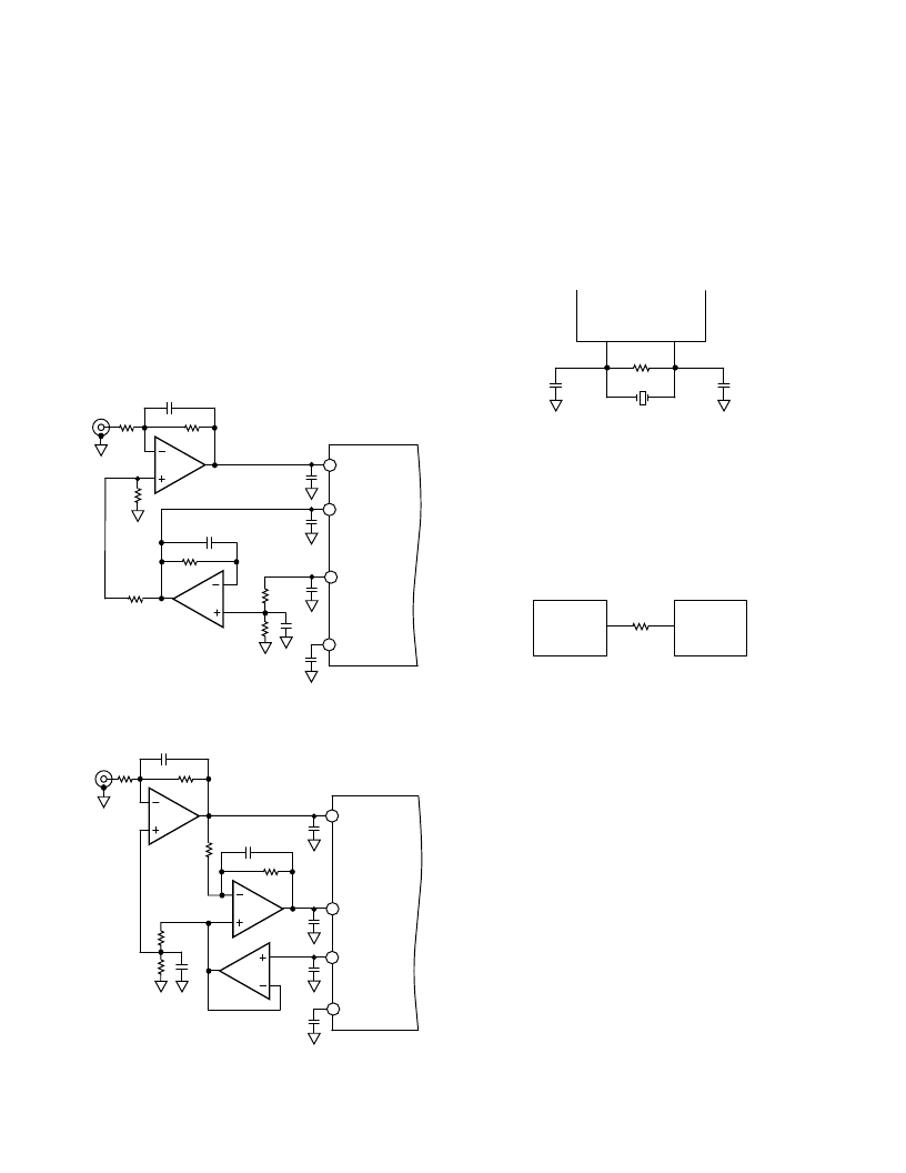
Input Circuits
Figures 34 and 35 show two simple circuits for bipolar mode
operation. Both circuits accept a single-ended bipolar signal
source and create the necessary differential signals at the input
to the ADC.
The circuit in Figure 34 creates a 0 V to 2.5 V signal at the
VIN(+) pin to form a differential signal around an initial bias of
1.25 V. For single-ended applications best THD performance is
obtained with VIN(–) set to 1.25 V rather than 2.5 V. The input
to the AD7722 can also be driven differentially with a comple-
mentary input as shown in Figure 35.
In this case, the input common-mode voltage is set to 2.5 V.
The 2.5 V p-p full-scale differential input is obtained with a
1.25 V p-p signal at each input in antiphase. This configuration
minimizes the required output swing from the amplifier circuit
and is useful for single supply applications.
12pF
1k
1k
1k
12pF
1k
100nF
374k
1nF
VIN(–)
1/2
OP275
VIN(+)
18
REF1
22
REF2
100nF
24
AD7722
DIFFERENTIAL
INPUT = 2.5V p-p
VIN(–) BIAS
VOLTAGE = 1.25V
AIN =
±
1.25V
16
1/2
OP275
1k
374k
10nF
1nF
Figure 34. Single-Ended Analog Input Circuit for Bipolar
Mode Operation
12pF
1k
AIN =
±
0.625V
1k
1k
12pF
1k
1/2
OP275
100nF
R
R
1nF
VIN(–)
1nF
1/2
OP275
16
VIN(+)
18
DIFFERENTIAL
INPUT = 2.5V p-p
COMMON MODE
VOLTAGE = 2.5V
REF1
22
OP07
REF2
100nF
24
AD7722
Figure 35. Single-Ended to Differential Analog Input
Circuit for Bipolar Mode Operation
The 1 nF capacitors at each ADC input store charge to aid the
amplifier settling as the input is continuously sampled. A
resistor in series with the drive amplifier output and the 1 nF
input capacitor may also be used to create an antialias filter.
Clock Generation
The AD7722 contains an oscillator circuit to allow a crystal or
an external clock signal to generate the master clock for the
ADC. The connection diagram for use with crystal is shown in
Figure 36, below. Consult the crystal manufacturer’s recom-
mendation for the load capacitors.
1M
XTAL
CLKIN
AD7722
Figure 36. Crystal Oscillator Connection
An external clock must be free of ringing and have a minimum
rise time of 5 ns. Degradation in performance can result, as high
edge rates increase coupling that can generate noise in the
sampling process. The connection diagram for an external clock
source (Figure 37) shows a series damping resistor connected
between the clock output and the clock input to the AD7722.
The optimum resistor will depend on the board layout and the
impedance of the trace connecting to the clock input.
CLOCK
CIRCUITRY
CLKIN
AD7722
25–150
Figure 37. External Clock Oscillator Connection
A low phase-noise clock should be used to generate the ADC
sampling clock because sampling clock jitter effectively modu-
lates the input signal and raises the noise floor. The sampling
clock generator should be isolated from noisy digital circuits,
grounded and heavily decoupled to the analog ground plane.
The sampling clock generator should be referenced to the
analog ground plane in a split-ground system. However, this is
not always possible because of system constraints. In many
cases, the sampling clock must be derived from a higher
frequency multipurpose system clock that is generated on the
digital ground plane. If the clock signal is passed between its
origin on a digital ground plane to the AD7722 on the analog
ground plane, the ground noise between the two planes adds
directly to the clock and will produce excess jitter. The jitter can
cause degradation in the signal-to-noise ratio and also produce
unwanted harmonics.
This can be remedied somewhat by transmitting the sampling
clock signal as a differential one, using either a small RF trans-
former or a high speed differential driver and receiver such as
PECL. In either case, the original master system clock should be
generated from a low phase noise crystal oscillator.
相關PDF資料 |
PDF描述 |
|---|---|
| AD7723 | 16-Bit, 1.2 MSPS CMOS, Sigma-Delta ADC |
| AD7723BS | 16-Bit, 1.2 MSPS CMOS, Sigma-Delta ADC |
| AD7724AST | Dual CMOS Modulators |
| AD7724 | Dual CMOS Modulators |
| AD7725 | 16-Bit 900 kSPS ADC with a Programmable Postprocessor |
相關代理商/技術參數 |
參數描述 |
|---|---|
| AD7722AS-ES | 制造商:Rochester Electronics LLC 功能描述:- Bulk |
| AD7722ASZ | 功能描述:IC ADC 16BIT 195KSPS 44-MQFP RoHS:是 類別:集成電路 (IC) >> 數據采集 - 模數轉換器 系列:- 標準包裝:1 系列:- 位數:14 采樣率(每秒):83k 數據接口:串行,并聯 轉換器數目:1 功率耗散(最大):95mW 電壓電源:雙 ± 工作溫度:0°C ~ 70°C 安裝類型:通孔 封裝/外殼:28-DIP(0.600",15.24mm) 供應商設備封裝:28-PDIP 包裝:管件 輸入數目和類型:1 個單端,雙極 |
| AD7722CSZ | 制造商:Analog Devices 功能描述: |
| AD7723 | 制造商:AD 制造商全稱:Analog Devices 功能描述:16-Bit, 1.2 MSPS CMOS, Sigma-Delta ADC |
| AD7723BS | 制造商:Analog Devices 功能描述:ADC Single Delta-Sigma 19.2Msps 16-bit Parallel/Serial 44-Pin MQFP 制造商:Analog Devices 功能描述:Analog-Digital Converter IC Number of Bi |
發布緊急采購,3分鐘左右您將得到回復。