- 您現在的位置:買賣IC網 > PDF目錄373920 > AD7851KR (ANALOG DEVICES INC) 14-Bit 333 kSPS Serial A/D Converter PDF資料下載
參數資料
| 型號: | AD7851KR |
| 廠商: | ANALOG DEVICES INC |
| 元件分類: | ADC |
| 英文描述: | 14-Bit 333 kSPS Serial A/D Converter |
| 中文描述: | 1-CH 14-BIT SUCCESSIVE APPROXIMATION ADC, SERIAL ACCESS, PDSO24 |
| 封裝: | MS-013AD, SOIC-24 |
| 文件頁數: | 14/36頁 |
| 文件大小: | 435K |
| 代理商: | AD7851KR |
第1頁第2頁第3頁第4頁第5頁第6頁第7頁第8頁第9頁第10頁第11頁第12頁第13頁當前第14頁第15頁第16頁第17頁第18頁第19頁第20頁第21頁第22頁第23頁第24頁第25頁第26頁第27頁第28頁第29頁第30頁第31頁第32頁第33頁第34頁第35頁第36頁
AD7851
–14–
REV. A
CIRCUIT INFORMAT ION
T he AD7851 is a fast, 14-bit single supply A/D converter. T he
part requires an external 6/7 MHz master clock (CLK IN), two
C
REF
capacitors, a
CONVST
signal to start conversion and
power supply decoupling capacitors. T he part provides the user
with track/hold, on-chip reference, calibration features, A/D
converter and serial interface logic functions on a single chip.
T he A/D converter section of the AD7851 consists of a conven-
tional successive-approximation converter based around a ca-
pacitor DAC. T he AD7851 accepts an analog input range of
0 V to +V
DD
where the reference can be tied to V
DD
. T he refer-
ence input to the part is buffered onchip.
A major advantage of the AD7851 is that a conversion can be
initiated in software as well as applying a signal to the
CONVST
pin. Another innovative feature of the AD7851 is self-calibration
on power-up, which is initiated having a 0.01
μ
F capacitor from
the
CAL
pin to AGND, to give superior dc accuracy. T he part
should be allowed 150 ms after power-up to perform this auto-
matic calibration before any reading or writing takes place. T he
part is available in a 24-pin SSOP package and this offers the user
considerable space saving advantages over alternative solutions.
CONVE RT E R DE T AILS
T he master clock for the part must be applied to the CLK IN
pin. Conversion is initiated on the AD7851 by pulsing the
CONVST
input or by writing to the control register and setting
the
CONVST
bit to 1. On the rising edge of
CONVST
(or at
the end of the control register write operation), the on-chip
track/hold goes from track to hold mode. T he falling edge of the
CLK IN signal which follows the rising edge of the edge of
CONVST
signal initiates the conversion, provided the rising
edge of
CONVST
occurs at least 10 ns typically before this
CLK IN edge. T he conversion cycle will take 18.5 CLK IN peri-
ods from this CLK IN falling edge. If the 10 ns setup time is
AV
DD
DV
DD
AIN(+)
AIN(–)
AMODE
C
REF1
C
REF2
SLEEP
DIN
DOUT
SYNC
SM1
SM2
CONVST
AGND
DGND
CLKIN
SCLK
REF
IN
/REF
OUT
POLARITY
AD7851
ANALOG (5V)
SUPPLY
0.01μF
0.1μF
10μF
DV
DD
UNIPOLAR RANGE
0.01μF
47nF
SERIAL MODE
SELECTION BITS
MASTER
CLOCK
INPUT
CONVERSION
START INPUT
FRAME SYNC OUTPUT
SERIAL DATA OUTPUT
0.01μF
CAL
AUTO CAL ON
POWER-UP
INTERNAL
REFERENCE
0V TO V
REF
INPUT
7MHz/6MHz
OSCILLATOR
SERIAL CLOCK OUTPUT
DV
DD
333kHz/285kHz PULSE
GENERATOR
OPTIONAL
EXTERNAL
REFERENCE
AD1584/REF198
0.01μF
ANALOG (5V)
SUPPLY
0.1μF
10μF
DIN AT DGND
=> NO WRITING
TO DEVICE
0.01μF
470nF
CH1
CH2
CH3
CH4
OSCILLOSCOPE
2 LEADING ZEROS
FOR ADC DATA
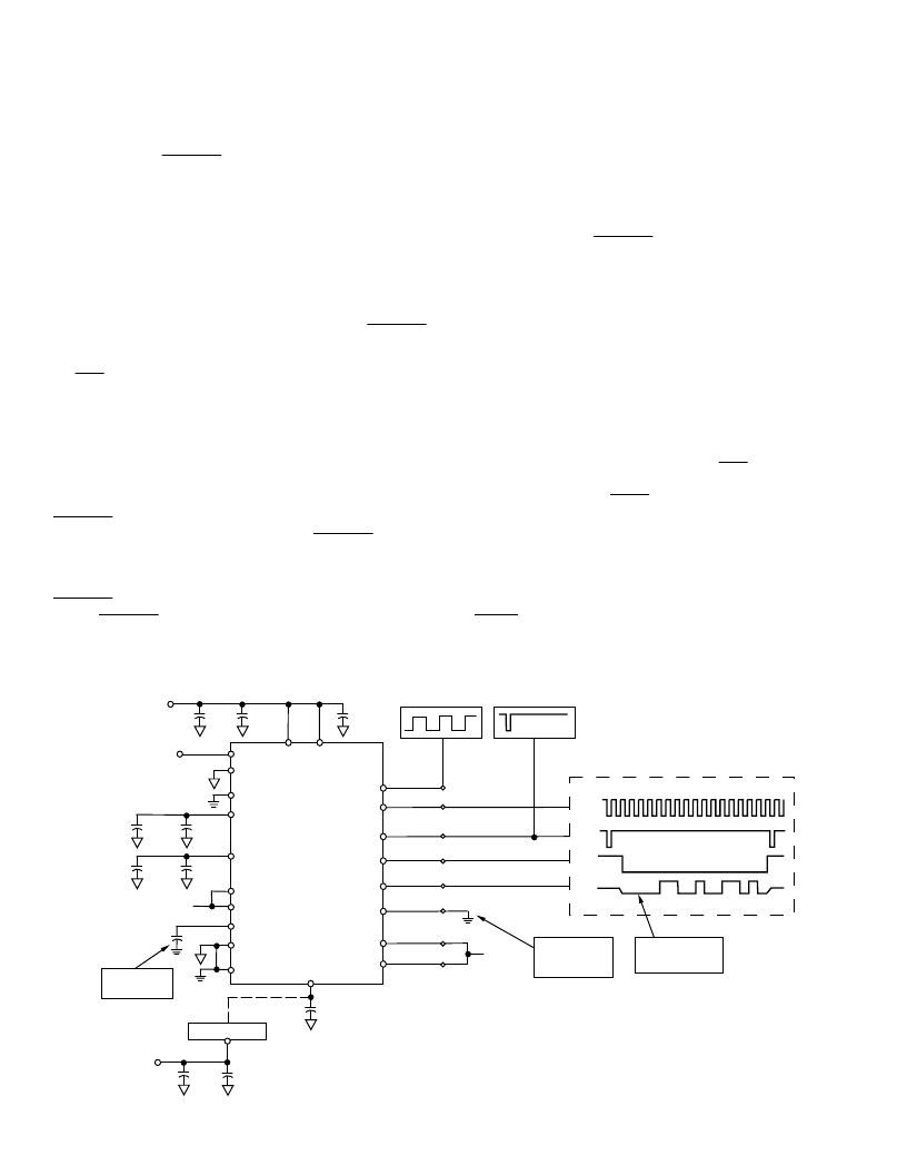
Figure 10. Typical Circuit
not met, the conversion will take 19.5 CLK IN periods. T he
maximum specified conversion time is 3.25
μ
s (6 MHz ) and
2.8
μ
s (7 MHz) for the A and K Grades respectively for the
AD7851 (19.5 t
CLK IN,
CLK IN = 6/7 MHz). When a conversion
is completed, the BUSY output goes low, and then the result of
the conversion can be read by accessing the data through the se-
rial interface. T o obtain optimum performance from the part,
the read operation should not occur during the conversion or
500 ns prior to the next
CONVST
rising edge. However, the
maximum throughput rates are achieved by reading/writing dur-
ing conversion, and reading/writing during conversion is likely
to degrade the Signal to (Noise + Distortion) by only 0.5 dBs. T he
AD7851 can operate at throughput rates up to 333 kHz. For the
AD7851 a conversion takes 19.5 CL K IN periods, 2 CL K IN
periods are needed for the acquisition time giving a full cycle
time of 3.59
μ
s (= 279 kHz, CLK IN = 6 MHz) for the K grade
and 3.08
μ
s (= 325 kHz, CLK IN = 7 MHz) for the A grade.
T Y PICAL CONNE CT ION DIAGRAM
Figure 10 shows a typical connection diagram for the AD7851.
T he DIN line is tied to DGND so that no data is written to the
part. T he AGND and the DGND pins are connected together
at the device for good noise suppression. T he
CAL
pin has a
0.01
μ
F capacitor to enable an automatic self-calibration on
power-up. T he SCLK and
SYNC
are configured as outputs by
having SM1 and SM2 at DV
DD
. T he conversion result is output
in a 16-bit word with 2 leading zeros followed by the MSB of
the 14-bit result. Note that after the AV
DD
and DV
DD
power-up,
the part will require 150 ms for the internal reference to settle
and for the automatic calibration on power-up to be completed.
For applications where power consumption is a major concern,
the
SLEEP
pin can be connected to DGND. See Power-Down
section for more detail on low power applications.
相關PDF資料 |
PDF描述 |
|---|---|
| AD7853LARS | 3 V to 5 V Single Supply, 200 kSPS 12-Bit Sampling ADCs |
| AD7853L* | Single Supply V.35 Transceiver; Package: SO; No of Pins: 28; Temperature Range: -40°C to +85°C |
| AD7853L | 3 V to 5 V Single Supply, 200 kSPS 12-Bit Sampling ADCs(單電源,200kSPS 12位采樣A/D轉換器) |
| AD7853 | 3 V to 5 V Single Supply, 200 KSPS 12-Bit Sampling ADCs(單電源,200kSPS 12位采樣A/D轉換器) |
| AD7853AN | 3 V to 5 V Single Supply, 200 kSPS 12-Bit Sampling ADCs |
相關代理商/技術參數 |
參數描述 |
|---|---|
| AD7851KR-REEL | 制造商:Analog Devices 功能描述: |
| AD7851KRZ | 功能描述:IC ADC 14BIT SRL 333KSPS 24-SOIC RoHS:是 類別:集成電路 (IC) >> 數據采集 - 模數轉換器 系列:- 標準包裝:1,000 系列:- 位數:12 采樣率(每秒):300k 數據接口:并聯 轉換器數目:1 功率耗散(最大):75mW 電壓電源:單電源 工作溫度:0°C ~ 70°C 安裝類型:表面貼裝 封裝/外殼:24-SOIC(0.295",7.50mm 寬) 供應商設備封裝:24-SOIC 包裝:帶卷 (TR) 輸入數目和類型:1 個單端,單極;1 個單端,雙極 |
| AD7851KRZ3 | 制造商:AD 制造商全稱:Analog Devices 功能描述:14-Bit 333 kSPS Serial A/D Converter |
| AD7851KRZ-REEL | 功能描述:IC ADC 14BIT SRL 333KSPS 24-SOIC RoHS:是 類別:集成電路 (IC) >> 數據采集 - 模數轉換器 系列:- 標準包裝:1,000 系列:- 位數:12 采樣率(每秒):300k 數據接口:并聯 轉換器數目:1 功率耗散(最大):75mW 電壓電源:單電源 工作溫度:0°C ~ 70°C 安裝類型:表面貼裝 封裝/外殼:24-SOIC(0.295",7.50mm 寬) 供應商設備封裝:24-SOIC 包裝:帶卷 (TR) 輸入數目和類型:1 個單端,單極;1 個單端,雙極 |
| AD7851KRZ-REEL3 | 制造商:AD 制造商全稱:Analog Devices 功能描述:14-Bit 333 kSPS Serial A/D Converter |
發布緊急采購,3分鐘左右您將得到回復。