- 您現在的位置:買賣IC網 > PDF目錄373920 > AD7854L (Analog Devices, Inc.) 12-Bit Sampling ADC(單電源,200kSPS 12位采樣A/D轉換器) PDF資料下載
參數資料
| 型號: | AD7854L |
| 廠商: | Analog Devices, Inc. |
| 英文描述: | 12-Bit Sampling ADC(單電源,200kSPS 12位采樣A/D轉換器) |
| 中文描述: | 12位采樣ADC(單電源,速度高達200ksps的12位采樣的A / D轉換器) |
| 文件頁數: | 2/28頁 |
| 文件大小: | 268K |
| 代理商: | AD7854L |
第1頁當前第2頁第3頁第4頁第5頁第6頁第7頁第8頁第9頁第10頁第11頁第12頁第13頁第14頁第15頁第16頁第17頁第18頁第19頁第20頁第21頁第22頁第23頁第24頁第25頁第26頁第27頁第28頁
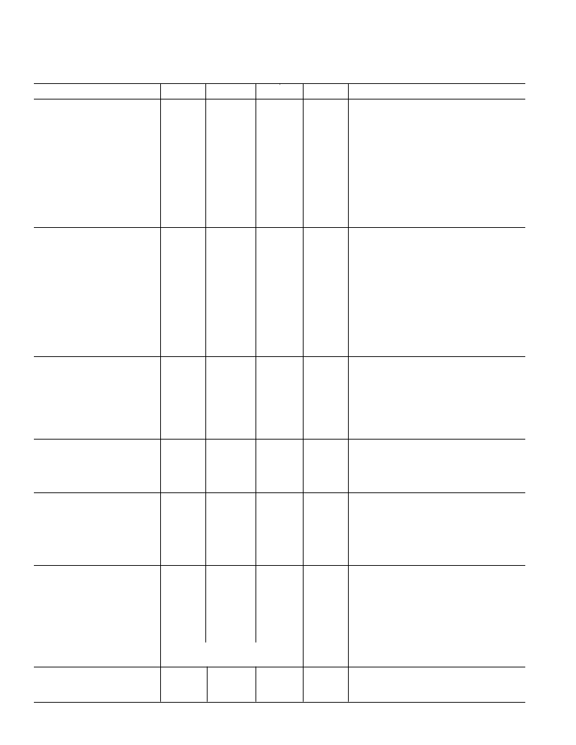
Parameter
A Version
1
B Version
1
S Version
1
Units
T est Conditions/Comments
DYNAMIC PERFORMANCE
Signal to Noise + Distortion Ratio
3
(SNR)
70
71
70
dB min
T ypically SNR is 72 dB
V
IN
= 10 kHz Sine Wave, f
SAMPLE
= 200 kHz
(100 kHz)
V
IN
= 10 kHz Sine Wave, f
SAMPLE
= 200 kHz
(100 kHz)
V
IN
= 10 kHz Sine Wave, f
SAMPLE
= 200 kHz
(100 kHz)
T otal Harmonic Distortion (T HD)
–78
–78
–78
dB max
Peak Harmonic or Spurious Noise
–78
–78
–78
dB max
Intermodulation Distortion (IMD)
Second Order T erms
–78
–78
–78
dB typ
fa = 9.983 kHz, fb = 10.05 kHz, f
SAMPLE
= 200 kHz
(100 kHz)
fa = 9.983 kHz, fb = 10.05 kHz, f
SAMPLE
= 200 kHz
(100 kHz)
T hird Order T erms
–78
–78
–78
dB typ
DC ACCURACY
Resolution
Integral Nonlinearity
Differential Nonlinearity
Unipolar Offset Error
12
±
1
±
1
±
3
±
2
±
4
±
2
±
4
±
2
±
4
±
2
±
4
12
±
0.5
±
1
±
3
±
2
±
4
±
2
±
4
±
2
±
4
±
2
±
4
12
±
1
±
1
±
4
±
2
±
4
±
2
±
5
±
2
±
5
±
2
±
5
Bits
LSB max
LSB max
LSB max
LSB typ
LSB max
LSB typ
LSB max
LSB typ
LSB max
LSB typ
LSB max
5 V Reference V
DD
= 5 V
Guaranteed No Missed Codes to 12 Bits
Unipolar Gain Error
Bipolar Positive Full-Scale Error
Negative Full-Scale Error
Bipolar Zero Error
ANALOG INPUT
Input Voltage Ranges
0 to V
REF
0 to V
REF
0 to V
REF
Volts
i.e., AIN(+) – AIN(–) = 0 to V
REF
, AIN(–) can be
biased up but AIN(+) cannot go below AIN(–).
i.e., AIN(+) – AIN(–) = –V
REF
/2 to +V
REF
/2, AIN(–)
should be biased to +V
REF
/2 and AIN(+) can go below
AIN(–) but cannot go below 0 V.
±
V
REF
/2
±
V
REF
/2
±
V
REF
/2
Volts
Leakage Current
Input Capacitance
±
1
20
±
1
20
±
1
20
μ
A max
pF typ
REFERENCE INPUT /OUT PUT
REF
IN
Input Voltage Range
Input Impedance
REF
OUT
Output Voltage
REF
OUT
T empco
2.3/V
DD
150
2.3/2.7
20
2.3/V
DD
150
2.3/2.7
20
2.3/V
DD
150
2.3/2.7
20
V min/max
k
typ
V min/max
ppm/
°
C typ
Functional from 1.2 V
LOGIC INPUT S
Input High Voltage, V
INH
3
2.1
0.4
0.6
±
10
10
3
2.1
0.4
0.6
±
10
10
3
2.1
0.4
0.6
±
10
10
V min
V min
V max
V max
μ
A max
pF max
AV
DD
= DV
DD
= 4.5 V to 5.5 V
AV
DD
= DV
DD
= 3.0 V to 3.6 V
AV
DD
= DV
DD
= 4.5 V to 5.5 V
AV
DD
= DV
DD
= 3.0 V to 3.6 V
T ypically 10 nA, V
IN
= 0 V or V
DD
Input Low Voltage, V
INL
Input Current, I
IN
Input Capacitance, C
IN4
LOGIC OUT PUT S
Output High Voltage, V
OH
I
SOURCE
= 200
μ
A
AV
DD
= DV
DD
= 4.5 V to 5.5 V
AV
DD
= DV
DD
= 3.0 V to 3.6 V
4
2.4
4
2.4
4
2.4
V min
V min
Output Low Voltage, V
OL
Floating-State Leakage Current
Floating-State Output Capacitance
4
Output Coding
0.4
±
10
10
0.4
±
10
10
0.4
±
10
10
V max
μ
A max
pF max
I
SINK
= 1.6 mA
Straight (Natural) Binary
T wos Complement
Unipolar Input Range
Bipolar Input Range
CONVERSION RAT E
Conversion T ime
T rack/Hold Acquisition T ime
t
CLK IN
×
18
(L Versions Only)
(L Versions Only)
4.5 (9)
0.5 (1)
4.5 (9)
0.5 (1)
4.5 (9)
0.5 (1)
μ
s max
μ
s min
AD7854/AD7854L–SPECIFICATIONS
1, 2
External Reference, f
CLKIN
= 4 MHz (1.8MHz for L Version); f
SAMPLE
= 200kHz (AD7854), 100kHz (AD7854L); T
A
= T
MN
to T
MAX
, unless otherwse
noted.) Specifications in () apply to the AD7854L.
(AV
DD
= DV
DD
= +3.0V to +5.5V, REF
IN
/REF
OUT
= 2.5 V
–2–
REV. 0
相關PDF資料 |
PDF描述 |
|---|---|
| AD7854 | 12-Bit Sampling ADC(單電源,200kSPS 12位采樣A/D轉換器) |
| AD7858LARS | 3 V to 5 V Single Supply, 200 kSPS 8-Channel, 12-Bit Sampling ADC |
| AD7858BN | 3 V to 5 V Single Supply, 200 kSPS 8-Channel, 12-Bit Sampling ADC |
| AD7858BR | 3 V to 5 V Single Supply, 200 kSPS 8-Channel, 12-Bit Sampling ADC |
| AD7858AN | 3 V to 5 V Single Supply, 200 kSPS 8-Channel, 12-Bit Sampling ADC |
相關代理商/技術參數 |
參數描述 |
|---|---|
| AD7854LAQ | 制造商:Rochester Electronics LLC 功能描述:12 BIT SINGLE CHANNEL PARALLEL ADC I.C. - Bulk |
| AD7854LAR | 制造商:Analog Devices 功能描述:ADC Single SAR 100ksps 12-bit Parallel 28-Pin SOIC W 制造商:Rochester Electronics LLC 功能描述:12-BIT SINGLE CHANNEL PARALLEL ADC I.C. - Bulk |
| AD7854LAR-REEL | 制造商:Analog Devices 功能描述:ADC Single SAR 100ksps 12-bit Parallel 28-Pin SOIC W T/R 制造商:Analog Devices 功能描述:ADC SGL SAR 100KSPS 12-BIT PARALLEL 28SOIC W - Tape and Reel |
| AD7854LARS | 功能描述:IC ADC 12BIT PARALLEL LP 28-SSOP RoHS:否 類別:集成電路 (IC) >> 數據采集 - 模數轉換器 系列:- 產品培訓模塊:Lead (SnPb) Finish for COTS Obsolescence Mitigation Program 標準包裝:2,500 系列:- 位數:12 采樣率(每秒):3M 數據接口:- 轉換器數目:- 功率耗散(最大):- 電壓電源:- 工作溫度:- 安裝類型:表面貼裝 封裝/外殼:SOT-23-6 供應商設備封裝:SOT-23-6 包裝:帶卷 (TR) 輸入數目和類型:- |
發布緊急采購,3分鐘左右您將得到回復。