- 您現在的位置:買賣IC網 > PDF目錄373920 > AD7854L (Analog Devices, Inc.) 12-Bit Sampling ADC(單電源,200kSPS 12位采樣A/D轉換器) PDF資料下載
參數資料
| 型號: | AD7854L |
| 廠商: | Analog Devices, Inc. |
| 英文描述: | 12-Bit Sampling ADC(單電源,200kSPS 12位采樣A/D轉換器) |
| 中文描述: | 12位采樣ADC(單電源,速度高達200ksps的12位采樣的A / D轉換器) |
| 文件頁數: | 24/28頁 |
| 文件大小: | 268K |
| 代理商: | AD7854L |
第1頁第2頁第3頁第4頁第5頁第6頁第7頁第8頁第9頁第10頁第11頁第12頁第13頁第14頁第15頁第16頁第17頁第18頁第19頁第20頁第21頁第22頁第23頁當前第24頁第25頁第26頁第27頁第28頁
AD7854/AD7854L
–24–
REV. 0
Resetting the Parallel Interface
If random data has been inadvertently written to the test regis-
ter, it is necessary to write the 16-bit word 0000 0000 0010
0000 (in two 8-bit bytes) to restore the test register to its default
value.
MICROPROCE SSOR INT E RFACING
T he parallel port on the AD7854/AD7854L allows the device to
be interfaced to microprocessors or DSP processors as a memory
mapped or I/O mapped device. T he
CS
and
RD
inputs are
common to all memory peripheral interfacing. T ypical inter-
faces to different processors are shown in Figures 38 to 41.
In all the interfaces shown, an external timer controls the
CONVST
input of the AD7854/AD7854L and the BUSY out-
put interrupts the host DSP. Also, the HBEN pin is connected
to address line A0 (X A0 in the case of the T MS320C30). T his
maps the AD7854/AD7854L to two locations in the processor
memory space, ADCaddr and ADCaddr+1. T hus when writing
to the ADC, first the 8 LSBs of the 16-bit are written to address
location ADCaddr and then the 8 MSBs to location ADCaddr+1.
All the interfaces use a 12-bit data bus, so only one read is needed
from location ADCaddr to access the ADC output data register
or the status register. T o read from the other registers, the
8 MSBs must be read from location ADCaddr+1. Interfacing
to 8-bit bus systems is similar, except that two reads are
required to obtain data from all the registers.
AD7854/AD7854L to ADSP-21xx
Figure 38 shows the AD7854/AD7854L interfaced to the
ADSP-21xx series of DSPs as a memory mapped device. A
single wait state may be necessary to interface the AD7854/
AD7854L to the ADSP-21xx depending on the clock speed of
the DSP. T his wait state can be programmed via the data
memory waitstate control register of the ADSP-21xx (please see
ADSP-2100 Family Users Manual
for details). T he following
instruction reads data from the AD7854/AD7854L:
AX
0
= DM(ADCaddr)
Data can be written to the AD7854/AD7854L using the
instructions:
DM (ADCaddr) = AY
0
DM (ADCaddr+
1
) = AY
1
where
ADCaddr
is the address of the AD7854/AD7854L in
ADSP-21xx data memory,
AX
0 contains the data read from the
ADC, and
AY
0 contains the 8 LSBs and
AY
1 the 8 MSBs of
data written to the AD7854/AD7854L.
ADSP-21xx*
A13–A1
DMS
A0
WR
IRQ2
D23–D8
CS
HBEN
WR
RD
BUSY
DB11–DB0
AD7854/
AD7854L*
ADDR
DECODE
EN
ADDRESS BUS
DATA BUS
*ADDITIONAL PINS OMITTED FOR CLARITY
RD
Figure 38. AD7854/AD7854L to ADSP-21xx Parallel Interface
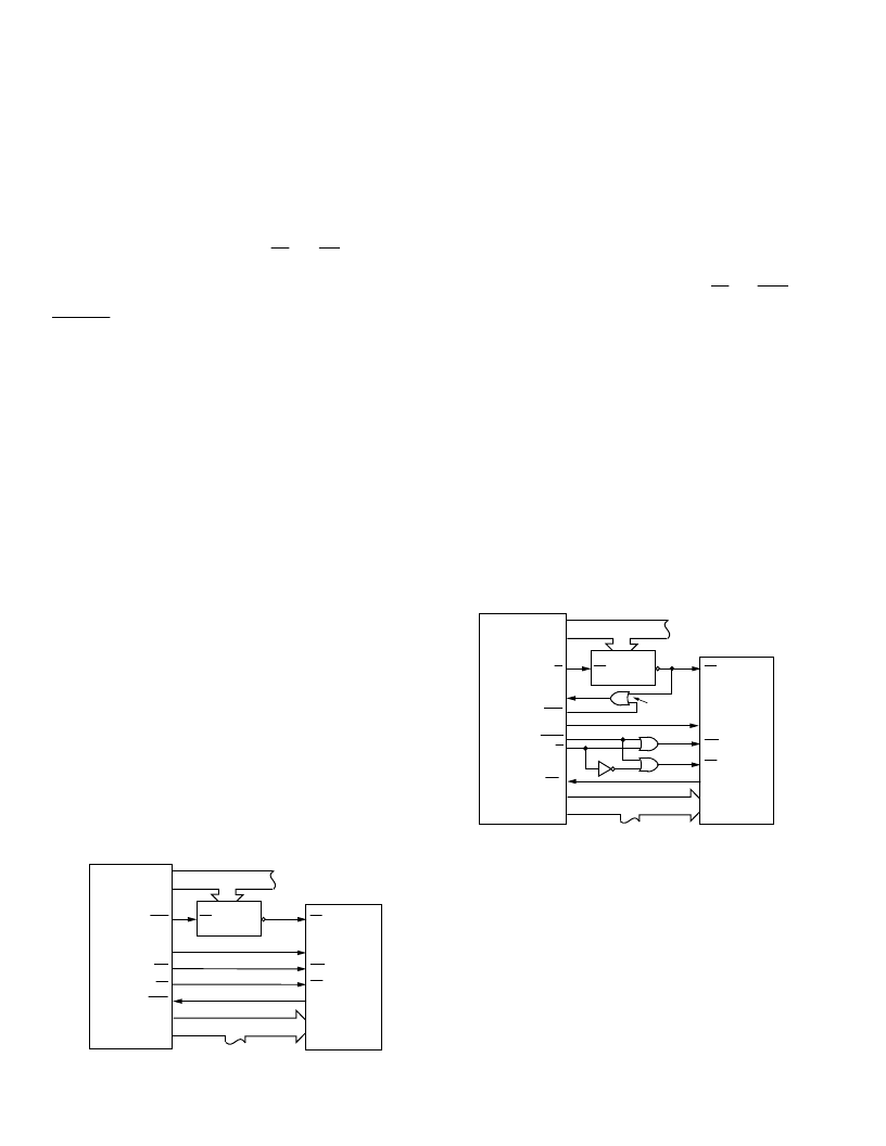
AD7854/AD7854L to T MS32020, T MS320C25 and T MS320C5x
A parallel interface between the AD7854/AD7854L and the
T MS32020, T MS320C25 and T MS320C5x family of DSPs are
shown in Figure 39. T he memory mapped addresses chosen for
the AD7854/AD7854L should be chosen to fall in the I/O
memory space of the DSPs.
T he parallel interface on the AD7854/AD7854L is fast enough
to interface to the T MS32020 with no extra wait states. In the
T MS320C25 interface, data accesses may be slowed sufficiently
when reading from and writing to the part to require the inser-
tion of one wait state. In such a case, this wait state can be gen-
erated using the single OR gate to combine the
CS
and
MSC
signals to drive the READY line of the T MS320C25, as shown
in Figure 39. Extra wait states are necessary when using the
T MS320C5x at their fastest clock speeds. Wait states can be
programmed via the IOWSR and CWSR registers (please see
T MS320C5x User Guide for details).
Data is read from the ADC using the following instruction:
IN D,ADCaddr
where
D
is the memory location where the data is to be stored
and
ADCaddr
is the I/O address of the AD7854/AD7854L.
Data is written to the ADC using the following two instructions:
OUT D
8
LSB, ADCaddr
OUT D
8
MSB, ADCaddr
+1
where
D
8
LSB
is the memory location where the 8 LSBs of data
are stored,
D
8
MSB
is the location where the 8 MSBs of data are
stored and
ADCaddr
and
ADCaddr
+1 are the I/O memory
spaces that the AD7854/AD7854L is mapped into.
TMS32020/
TMS320C25/
TMS320C50*
A15–A1
IS
READY
MSC
A0
STRB
R/
W
INT
x
D23–D0
TMS320C25
ONLY
CS
HBEN
WR
RD
BUSY
DB11–DB0
AD7854/
AD7854L*
ADDR
DECODE
EN
ADDRESS BUS
DATA BUS
*ADDITIONAL PINS OMITTED FOR CLARITY
Figure 39. AD7854/AD7854L to TMS32020/C25/C5x
Parallel Interface
相關PDF資料 |
PDF描述 |
|---|---|
| AD7854 | 12-Bit Sampling ADC(單電源,200kSPS 12位采樣A/D轉換器) |
| AD7858LARS | 3 V to 5 V Single Supply, 200 kSPS 8-Channel, 12-Bit Sampling ADC |
| AD7858BN | 3 V to 5 V Single Supply, 200 kSPS 8-Channel, 12-Bit Sampling ADC |
| AD7858BR | 3 V to 5 V Single Supply, 200 kSPS 8-Channel, 12-Bit Sampling ADC |
| AD7858AN | 3 V to 5 V Single Supply, 200 kSPS 8-Channel, 12-Bit Sampling ADC |
相關代理商/技術參數 |
參數描述 |
|---|---|
| AD7854LAQ | 制造商:Rochester Electronics LLC 功能描述:12 BIT SINGLE CHANNEL PARALLEL ADC I.C. - Bulk |
| AD7854LAR | 制造商:Analog Devices 功能描述:ADC Single SAR 100ksps 12-bit Parallel 28-Pin SOIC W 制造商:Rochester Electronics LLC 功能描述:12-BIT SINGLE CHANNEL PARALLEL ADC I.C. - Bulk |
| AD7854LAR-REEL | 制造商:Analog Devices 功能描述:ADC Single SAR 100ksps 12-bit Parallel 28-Pin SOIC W T/R 制造商:Analog Devices 功能描述:ADC SGL SAR 100KSPS 12-BIT PARALLEL 28SOIC W - Tape and Reel |
| AD7854LARS | 功能描述:IC ADC 12BIT PARALLEL LP 28-SSOP RoHS:否 類別:集成電路 (IC) >> 數據采集 - 模數轉換器 系列:- 產品培訓模塊:Lead (SnPb) Finish for COTS Obsolescence Mitigation Program 標準包裝:2,500 系列:- 位數:12 采樣率(每秒):3M 數據接口:- 轉換器數目:- 功率耗散(最大):- 電壓電源:- 工作溫度:- 安裝類型:表面貼裝 封裝/外殼:SOT-23-6 供應商設備封裝:SOT-23-6 包裝:帶卷 (TR) 輸入數目和類型:- |
發布緊急采購,3分鐘左右您將得到回復。